- 您現(xiàn)在的位置:買賣IC網(wǎng) > PDF目錄24691 > 05F8031 IC-SM-QUAD 12 BIT DAC PDF資料下載
參數(shù)資料
| 型號(hào): | 05F8031 |
| 英文描述: | IC-SM-QUAD 12 BIT DAC |
| 中文描述: | 集成電路釤四路12位DAC |
| 文件頁數(shù): | 1/12頁 |
| 文件大?。?/td> | 502K |
| 代理商: | 05F8031 |

REV. C
Information furnished by Analog Devices is believed to be accurate and
reliable. However, no responsibility is assumed by Analog Devices for its
use, nor for any infringements of patents or other rights of third parties
which may result from its use. No license is granted by implication or
otherwise under any patent or patent rights of Analog Devices.
a
Quad, 12-Bit DAC
Voltage Output with Readback
DAC8412/DAC8413
One Technology Way, P.O. Box 9106, Norwood, MA 02062-9106, U.S.A.
Tel: 617/329-4700
Fax: 617/326-8703
FUNCTIONAL BLOCK DIAGRAM
INPUT
REG A
OUTPUT
REG A
DAC A
A0
A1
DATA I/O
INPUT
REG B
INPUT
REG C
INPUT
REG D
OUTPUT
REG B
OUTPUT
REG C
OUTPUT
REG D
DAC B
DAC C
DAC D
CONTROL
LOGIC
I/O
PORT
R/W
CS
RESET
LDAC
DGND
12
V
LOGIC
V
DD
V
OUTA
V
OUTB
V
OUTC
V
OUTD
V
SS
V
REFH
V
REFL
FEATURES
+5 to
15 Volt Operation
Unipolar or Bipolar Operation
True Voltage Output
Double-Buffered Inputs
Reset to Min or Center Scale
Fast Bus Access Time
Readback
APPLICATIONS
Automatic Test Equipment
Digitally Controlled Calibration
Servo Controls
Process Control Equipment
GENERAL DESCRIPTION
The DAC8412 and DAC8413 are quad, 12-bit voltage output
DACs with readback capability. Built using a complementary
BiCMOS process, these monolithic DACs offer the user very
high package density.
Output voltage swing is set by the two reference inputs VREFH
and VREFL. By setting the VREFL input to 0 volts and VREFH to a
positive voltage, the DAC will provide a unipolar positive output
range. A similar configuration with VREFH at 0 volts and VREFL
at a negative voltage will provide a unipolar negative output
range. Bipolar outputs are configured by connecting both VREFH
and VREFL to nonzero voltages. This method of setting output
voltage range has advantages over other bipolar offsetting meth-
ods because it is not dependent on internal and external resis-
tors with different temperature coefficients.
Digital controls allow the user to load or read back data from
any DAC, load any DAC and transfer data to all DACs at one
time.
An active low RESET loads all DAC output registers to mid-
scale for the DAC8412 and zero scale for the DAC8413.
The DAC8412/DAC8413 are available in 28-pin plastic DIP,
cerdip, PLCC and LCC packages. They can be operated from
a wide variety of supply and reference voltages with supplies
ranging from single +5 volt to
±15 volts, and references from
+2.5 to
±10 volts. Power dissipation is less than 330 mW with
±15 volt supplies and only 60 mW with a +5 volt supply.
For MIL-STD-883 applications, contact your local ADI sales
office for the DAC8412/DAC8413/883 data sheet which speci-
fies operation over the –55
°C to +125°C temperature range. All
883 parts are also available on Standard Military Drawings
5962-91-76401MXA through -76404M3A.
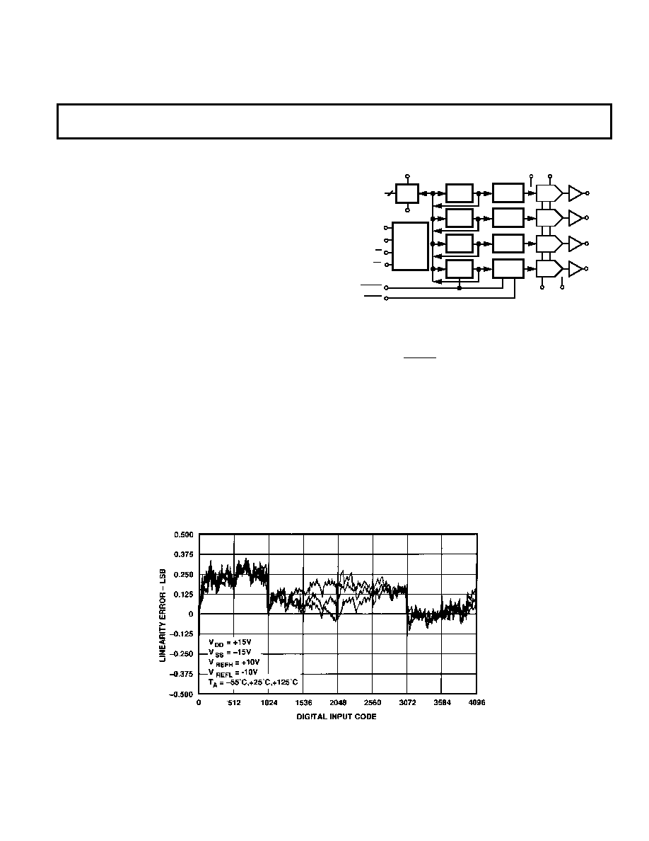
INL vs. Code Over Temperature
相關(guān)PDF資料 |
PDF描述 |
|---|---|
| 934051200112 | 40 MHz - 750 MHz RF/MICROWAVE WIDE BAND HIGH POWER AMPLIFIER |
| 934051230112 | 40 MHz - 750 MHz RF/MICROWAVE WIDE BAND HIGH POWER AMPLIFIER |
| 934051510185 | 100 mA, 50 V, PNP, Si, SMALL SIGNAL TRANSISTOR |
| 934031080215 | 100 mA, 50 V, PNP, Si, SMALL SIGNAL TRANSISTOR, TO-236AB |
| 934051510115 | 100 mA, 50 V, PNP, Si, SMALL SIGNAL TRANSISTOR |
相關(guān)代理商/技術(shù)參數(shù) |
參數(shù)描述 |
|---|---|
| 05FD101J03 | 制造商: 功能描述: 制造商:undefined 功能描述: |
| 05FD111J03 | 制造商: 功能描述: 制造商:undefined 功能描述: |
| 05FD161J03 | 制造商: 功能描述: 制造商:undefined 功能描述: |
| 05FD241J03 | 制造商: 功能描述: 制造商:undefined 功能描述: |
| 05FD271J03 | 制造商: 功能描述: 制造商:undefined 功能描述: |
發(fā)布緊急采購,3分鐘左右您將得到回復(fù)。