- 您現(xiàn)在的位置:買賣IC網(wǎng) > PDF目錄376460 > XRT4000 (Exar Corporation) Universal Multiprotocol Serial Interface PDF資料下載
參數(shù)資料
| 型號: | XRT4000 |
| 廠商: | Exar Corporation |
| 英文描述: | Universal Multiprotocol Serial Interface |
| 中文描述: | 通用多協(xié)議串行接口 |
| 文件頁數(shù): | 13/46頁 |
| 文件大小: | 396K |
| 代理商: | XRT4000 |
第1頁第2頁第3頁第4頁第5頁第6頁第7頁第8頁第9頁第10頁第11頁第12頁當前第13頁第14頁第15頁第16頁第17頁第18頁第19頁第20頁第21頁第22頁第23頁第24頁第25頁第26頁第27頁第28頁第29頁第30頁第31頁第32頁第33頁第34頁第35頁第36頁第37頁第38頁第39頁第40頁第41頁第42頁第43頁第44頁第45頁第46頁
XRT4000
Rev. 1.00
- 13 -
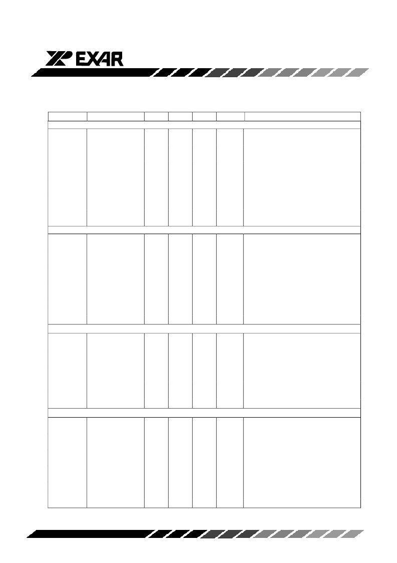
ELECTRICAL CHARCTERISTICS (CONT’D)
Test Conditions: VDD = 5V, VSS = -6V, VPP = 12V (all
±
5%), TA = 25
°
C
Symbol
V.10 Driver
V
O
Parameter
Min
Typ
Max
Units
Conditions
Output Voltage
±4.0
±3.6
±6.0
V
V
mA
Open Circuit, RL = 3.9k
RL = 450
(Figure 9)
VO = GND
I
SS
Short-Circuit
Current
Input Leakage
Current
Rise or Fall Time
±100
I
OZ
±0.1
±100
μ
A
-0.25
≤
VO
≤
0.25V, Power Off or
Driver Disabled
(Figures 9, 13), RL = 450
, CL = 100pF
RSLEW_CNTL = 10k
(Figures 9, 13), RL = 450
, CL = 100pF
RSLEW_CNTL = 10k
(Figures 9, 13), RL = 450
, CL = 100pF
RSLEW_CNTL = 10k
t
r
, t
f
0
5
μ
s
T
PLH
Input to output
5
μ
s
T
PHL
Input to output
5
μ
s
V.10 Receiver
V
TH
Receiver Input
Threshold Voltage
Receiver Input
Hysteresis
Receiver Input
Current
Receiver Input
Impedance
Rise or Fall Time
Input to Output
Input to Output
-0.2
0.2
V
AV
TH
35
60
mV
I
IN
±1
±1.5
mA
-10
≤
VA
≤
10V
R
IN
9
10
11
k
-10
≤
VA
≤
10V
t
r
, t
f
T
PLH
T
PHL
20
100
100
ns
ns
ns
(Figures 10, 14)
(Figures 10, 14)
(Figures 10, 14)
V.28 Driver
V
O
Output Voltage
±5
±5.5
±6
V
Open Circuit
RL = 3k (Figure 9)
VO = GND
I
SS
Short-Circuit
Current
Input Leakage
Current
Slew Rate
Input to output
Input to output
±100
mA
I
OZ
±0.01
±100
μ
A
-0.25
≤
VCM
≤
0.25V, Power Off or
Driver Disabled
(Figures 9, 13), RL = 3k, CL = 2500pF
(Figures 9, 13), RL = 3k, CL = 2500pF
(Figures 9, 13), RL = 3k, CL = 2500pF
SR
T
PLH
T
PHL
4.0
30.0
4
4
V/
μ
s
μ
s
μ
s
2
2
V.28 Receiver
V
THL
Input Low
Threshold Voltage
Input High
Threshold Voltage
Receiver Input
Hysteresis
Receiver Input
Impedance
Rise or Fall Time
Input to Output
Input to Output
1.4
0.8
V
V
TLH
2.0
1.4
V
AV
TH
0.1
0.4
1.0
V
R
IN
3
5
7
k
-15
≤
VA
≤
15V
t
r
, t
f
T
PLH
T
PHL
20
120
180
ns
ns
ns
(Figures 10, 14)
(Figures 10, 14)
(Figures 10, 14)
相關(guān)PDF資料 |
PDF描述 |
|---|---|
| XRT4500 | MULTIPROTOCOL SERIAL NETWORK INTERFACE IC |
| XRT4500CV | MULTIPROTOCOL SERIAL NETWORK INTERFACE IC |
| XRT56L85 | Low Power PCM Line Interface |
| XRT5794ES | Evaluation System |
| XRT5894ES | () |
相關(guān)代理商/技術(shù)參數(shù) |
參數(shù)描述 |
|---|---|
| XRT4000CV | 制造商:未知廠家 制造商全稱:未知廠家 功能描述:Transceiver |
| XR-T445B | 制造商:未知廠家 制造商全稱:未知廠家 功能描述:Telecommunication IC |
| XRT4500 | 制造商:EXAR 制造商全稱:EXAR 功能描述:MULTIPROTOCOL SERIAL NETWORK INTERFACE IC |
| XRT4500CV | 制造商:EXAR 制造商全稱:EXAR 功能描述:MULTIPROTOCOL SERIAL NETWORK INTERFACE IC |
| XR-T5600P | 制造商:未知廠家 制造商全稱:未知廠家 功能描述:PCM Repeater |
發(fā)布緊急采購,3分鐘左右您將得到回復(fù)。