- 您現(xiàn)在的位置:買賣IC網(wǎng) > PDF目錄4176 > XC3130A-3PQ100C (Xilinx Inc)IC LOGIC CL ARRAY 3000GAT 100PQF PDF資料下載
參數(shù)資料
| 型號(hào): | XC3130A-3PQ100C |
| 廠商: | Xilinx Inc |
| 文件頁數(shù): | 27/76頁 |
| 文件大小: | 0K |
| 描述: | IC LOGIC CL ARRAY 3000GAT 100PQF |
| 產(chǎn)品變化通告: | XC4000XL/E, XC9500XV, XC3100A Discontinuance 12/Apr/2010 |
| 標(biāo)準(zhǔn)包裝: | 66 |
| 系列: | XC3000A/L |
| LAB/CLB數(shù): | 100 |
| RAM 位總計(jì): | 22176 |
| 輸入/輸出數(shù): | 80 |
| 門數(shù): | 2000 |
| 電源電壓: | 4.25 V ~ 5.25 V |
| 安裝類型: | 表面貼裝 |
| 工作溫度: | 0°C ~ 85°C |
| 封裝/外殼: | 100-BQFP |
| 供應(yīng)商設(shè)備封裝: | 100-QFP(14x20) |
| 其它名稱: | 122-1041 |
第1頁第2頁第3頁第4頁第5頁第6頁第7頁第8頁第9頁第10頁第11頁第12頁第13頁第14頁第15頁第16頁第17頁第18頁第19頁第20頁第21頁第22頁第23頁第24頁第25頁第26頁當(dāng)前第27頁第28頁第29頁第30頁第31頁第32頁第33頁第34頁第35頁第36頁第37頁第38頁第39頁第40頁第41頁第42頁第43頁第44頁第45頁第46頁第47頁第48頁第49頁第50頁第51頁第52頁第53頁第54頁第55頁第56頁第57頁第58頁第59頁第60頁第61頁第62頁第63頁第64頁第65頁第66頁第67頁第68頁第69頁第70頁第71頁第72頁第73頁第74頁第75頁第76頁

R
November 9, 1998 (Version 3.1)
7-35
XC3000 Series Field Programmable Gate Arrays
7
Device Performance
The XC3000 families of FPGAs can achieve very high per-
formance. This is the result of
A sub-micron manufacturing process, developed and
continuously being enhanced for the production of
state-of-the-art CMOS SRAMs.
Careful optimization of transistor geometries, circuit
design, and lay-out, based on years of experience with
the XC3000 family.
A look-up table based, coarse-grained architecture that
can collapse multiple-layer combinatorial logic into a
single function generator. One CLB can implement up
to four layers of conventional logic in as little as 1.5 ns.
Actual system performance is determined by the timing of
critical paths, including the delay through the combinatorial
and sequential logic elements within CLBs and IOBs, plus
the delay in the interconnect routing. The AC-timing speci-
fications state the worst-case timing parameters for the var-
ious logic resources available in the XC3000-families
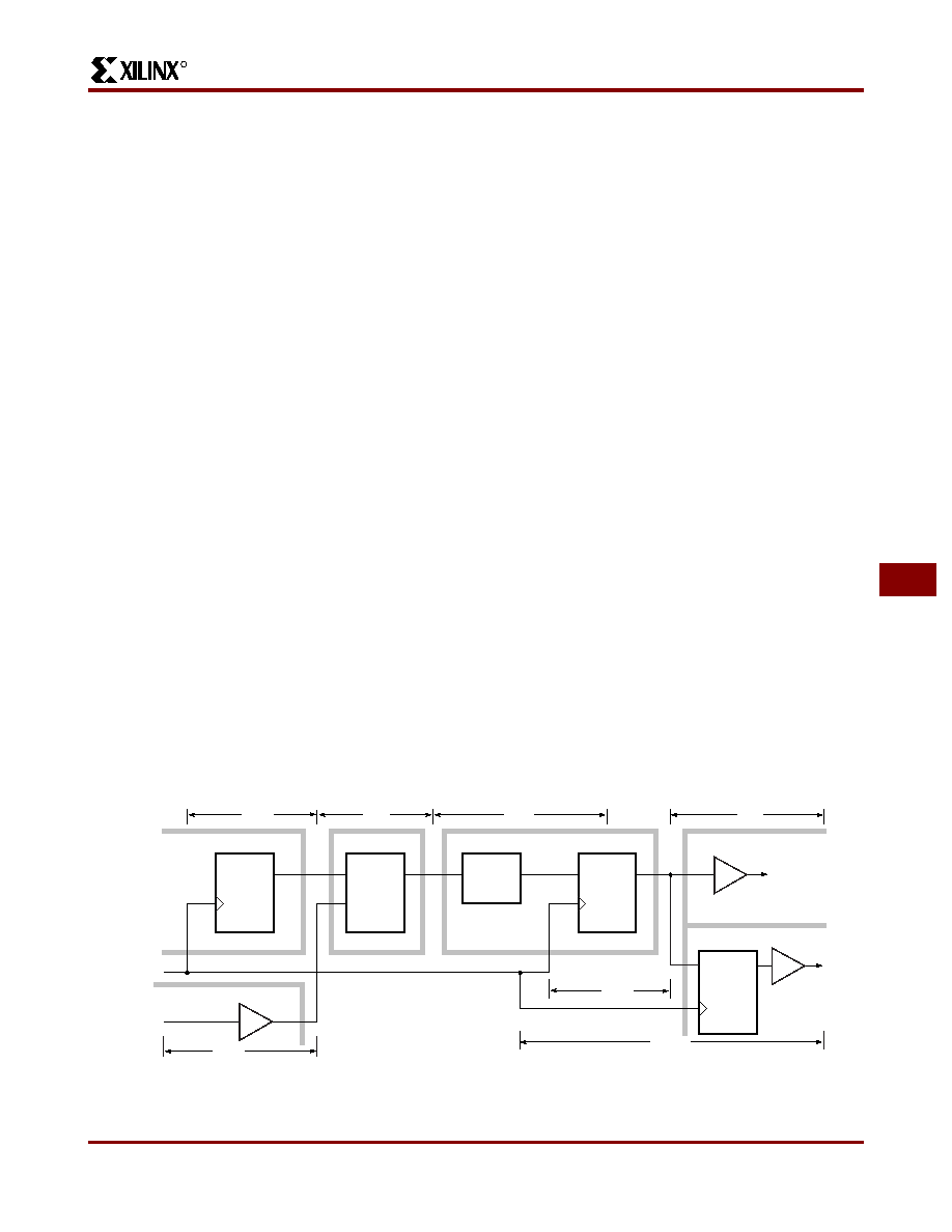
architecture. Figure 31 shows a variety of elements
involved in determining system performance.
Logic block performance is expressed as the propagation
time from the interconnect point at the input to the block to
the output of the block in the interconnect area. Since com-
binatorial logic is implemented with a memory lookup table
within a CLB, the combinatorial delay through the CLB,
called TILO, is always the same, regardless of the function
being implemented. For the combinatorial logic function
driving the data input of the storage element, the critical
timing is data set-up relative to the clock edge provided to
the flip-flop element. The delay from the clock source to the
output of the logic block is critical in the timing signals pro-
duced by storage elements. Loading of a logic-block output
is limited only by the resulting propagation delay of the
larger interconnect network. Speed performance of the
logic block is a function of supply voltage and temperature.
See Figure 32.
Interconnect
performance
depends
on
the
routing
resources used to implement the signal path. Direct inter-
connects to the neighboring CLB provide an extremely fast
path. Local interconnects go through switch matrices
(magic boxes) and suffer an RC delay, equal to the resis-
tance of the pass transistor multiplied by the capacitance of
the driven metal line. Longlines carry the signal across the
length or breadth of the chip with only one access delay.
Generous on-chip signal buffering makes performance rel-
atively insensitive to signal fan-out; increasing fan-out from
1 to 8 changes the CLB delay by only 10%. Clocks can be
distributed with two low-skew clock distribution networks.
The tools in the Development System used to place and
route a design in an XC3000 FPGA automatically calculate
the actual maximum worst-case delays along each signal
path. This timing information can be back-annotated to the
design’s netlist for use in timing simulation or examined
with, a static timing analyzer.
Actual system performance is applications dependent. The
maximum clock rate that can be used in a system is deter-
mined by the critical path delays within that system. These
delays are combinations of incremental logic and routing
delays, and vary from design to design. In a synchronous
system, the maximum clock rate depends on the number of
combinatorial
logic
layers
between
re-synchronizing
flip-flops. Figure 33 shows the achievable clock rate as a
function of the number of CLB layers.
CLB
IOB
CLB
PAD
(K)
Logic
CKO
T
CLOCK
Clock to Output
Combinatorial
Setup
TCKO
TILO
TICK
(K)
PAD
IOB
TPID
TOKPO
OP
T
X3178
Figure 31: Primary Block Speed Factors. Actual timing is a function of various block factors combined with routing.
factors. Overall performance can be evaluated with the timing calculator or by an optional simulation.
Product Obsolete or Under Obsolescence
相關(guān)PDF資料 |
PDF描述 |
|---|---|
| XC3130A-3PC84C | IC LOGIC CL ARRAY 3000GAT 84PLCC |
| RCB108DHBR | CONN EDGECARD 216PS R/A .050 DIP |
| XC3120A-3PC68C | IC LOGIC CL ARRAY 2000GAT 68PLCC |
| ASC49DRYN-S93 | CONN EDGECARD 98POS DIP .100 SLD |
| XC3090A-7PC84C | IC LOGIC CL ARRAY 9000GAT 84PLCC |
相關(guān)代理商/技術(shù)參數(shù) |
參數(shù)描述 |
|---|---|
| XC3130A-3PQ100C0262 | 制造商:Xilinx 功能描述: |
| XC3130A-3PQ100I | 制造商:Xilinx 功能描述: |
| XC3130A-3VQ100C | 制造商:Xilinx 功能描述: |
| XC3130A-3VQ100I | 制造商:XILINX 制造商全稱:XILINX 功能描述:Field Programmable Gate Arrays (XC3000A/L, XC3100A/L) |
| XC3130A-3VQ64C | 制造商:XILINX 制造商全稱:XILINX 功能描述:Field Programmable Gate Arrays (XC3000A/L, XC3100A/L) |
發(fā)布緊急采購,3分鐘左右您將得到回復(fù)。