- 您現(xiàn)在的位置:買(mǎi)賣(mài)IC網(wǎng) > PDF目錄372532 > X25385 Selectable Timeout Watchdog & V CC Supervisory Circuit w/Serial E 3 PROM(可選超時(shí)看門(mén)狗監(jiān)控電路) PDF資料下載
參數(shù)資料
| 型號(hào): | X25385 |
| 英文描述: | Selectable Timeout Watchdog & V CC Supervisory Circuit w/Serial E 3 PROM(可選超時(shí)看門(mén)狗監(jiān)控電路) |
| 中文描述: | 可選的超時(shí)看門(mén)狗 |
| 文件頁(yè)數(shù): | 1/15頁(yè) |
| 文件大?。?/td> | 90K |
| 代理商: | X25385 |
當(dāng)前第1頁(yè)第2頁(yè)第3頁(yè)第4頁(yè)第5頁(yè)第6頁(yè)第7頁(yè)第8頁(yè)第9頁(yè)第10頁(yè)第11頁(yè)第12頁(yè)第13頁(yè)第14頁(yè)第15頁(yè)

7064 1 0 2/4/98 T0/C0/D0 SH
Xicor, Inc. 1994, 1995, 1996 Patents Pending
1
Characteristics subject to change without notice
8K
X25383/85
1K x 8 Bit
Selectable Timeout Watchdog & V
CC
Supervisory Circuit w/Serial E
2
PROM
FEATURES
Selectable Timeout Watchdog Timer
Low Vcc Detection and Reset Assertion
—Reset Signal Valid to Vcc=1V
Save Critical Data With IDLock Memory
—IDLock First or Last Page, any 1/4 or Lower 1/2
of E
PROM Array
Long Battery Life With Low Power Consumption
—<50
μ
A Max Standby Current, Watchdog On
—<1
μ
A Max Standby Current, Watchdog Off
—<3mA Max Active Current during Write
—<400
μ
A Max Active Current during Read
1.8V to 3.6V, 2.7V to 5.5V and 4.5V to 5.5V Power
Supply Versions
5MHz Clock Rate
Minimize Programming Time
—16 Byte Page Write Mode
—Self-Timed Write Cycle
—5ms Write Cycle Time (Typical)
SPI Modes (0,0 & 1,1)
Built-in Inadvertent Write Protection
—Power-Up/Power-Down Protection Circuitry
—Write Enable Latch
—Write Protect Pin
High Reliability
Available Packages
—8-Lead TSSOP
—8-Lead SOIC
2
DESCRIPTION
These devices combine three popular functions, Watch-
dog Timer, Supply Voltage Supervision, and Serial
E
PROM Memory in one package. This combination low-
ers system cost, reduces board space requirements, and
increases reliability.
2
The Watchdog Timer provides an independent protection
mechanism for microcontrollers. During a system failure,
the device will respond with a RESET/RESET signal
after a selectable time-out interval. The user selects the
interval from three preset values. Once selected, the
interval does not change, even after cycling the power.
The user’s system is protected from low voltage condi-
tions by the device’s low Vcc detection circuitry. When
Vcc falls below the minimum Vcc trip point, the system is
reset. RESET/RESET is asserted until Vcc returns to
proper operating levels and stabilizes.
The memory portion of the device is a CMOS Serial
E
PROM array with Xicor’s IDLock Memory. The array is
internally organized as x 8. The device features a Serial
Peripheral Interface (SPI) and software protocol allowing
operation on a simple four-wire bus.
2
The device utilizes Xicor’s proprietary Direct Write
providing a minimum endurance of 100,000 cycles per
sector and a minimum data retention of 100 years.
TM
cell,
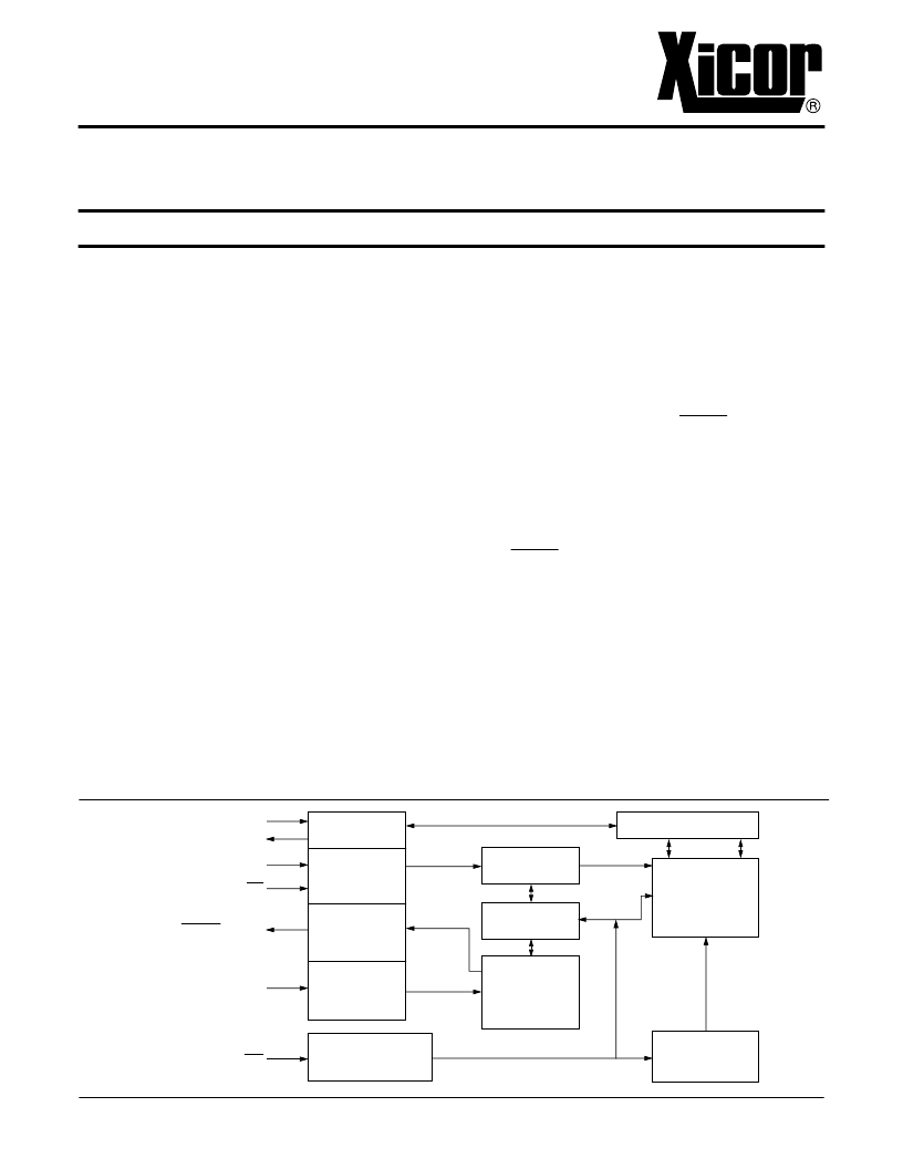
BLOCK DIAGRAM
DATA
REGISTER
COMMAND
DECODE &
CONTROL
LOGIC
RESET
CONTROL
LOW
VOLTAGE
SENSE
WRITE
CONTROL
X - DECODE
LOGIC
STATUS
REGISTER
WATCHDOG
TIMER
PAGE DECODE LOGIC
SERIAL
E
PROM
ARRAY
2
HIGH
VOLTAGE
CONTROL
SI
SO
SCK
CS
RESET/RESET
V
CC
WP
7036 FRM 01
16
8
相關(guān)PDF資料 |
PDF描述 |
|---|---|
| X25640S | IC-SM-64K SERIAL EEPROM+SPI |
| X25330S8 | SPI Serial EEPROM |
| X25330S8I | SPI Serial EEPROM |
| X25330S8I-2.5 | SPI Serial EEPROM |
| X25640 | Advanced SPI Serial E2PROM With Block LockTM Protection |
相關(guān)代理商/技術(shù)參數(shù) |
參數(shù)描述 |
|---|---|
| X25385S8 | 制造商:未知廠家 制造商全稱(chēng):未知廠家 功能描述:SPI Serial EEPROM with Supervisory Features |
| X25385S8-1.8 | 制造商:未知廠家 制造商全稱(chēng):未知廠家 功能描述:SPI Serial EEPROM with Supervisory Features |
| X25385S8-2.7 | 制造商:未知廠家 制造商全稱(chēng):未知廠家 功能描述:SPI Serial EEPROM with Supervisory Features |
| X25385S8I | 制造商:未知廠家 制造商全稱(chēng):未知廠家 功能描述:SPI Serial EEPROM with Supervisory Features |
| X25385S8I-1.8 | 制造商:未知廠家 制造商全稱(chēng):未知廠家 功能描述:SPI Serial EEPROM with Supervisory Features |
發(fā)布緊急采購(gòu),3分鐘左右您將得到回復(fù)。