- 您現(xiàn)在的位置:買賣IC網(wǎng) > PDF目錄372528 > X1242 Real Time Clock/Calendar/Alarms/CPU Supervisor(實時時鐘/日歷/鬧鐘/帶EEPROM的監(jiān)控) PDF資料下載
參數(shù)資料
| 型號: | X1242 |
| 英文描述: | Real Time Clock/Calendar/Alarms/CPU Supervisor(實時時鐘/日歷/鬧鐘/帶EEPROM的監(jiān)控) |
| 中文描述: | 實時時鐘/日歷/報警/ CPU監(jiān)控(實時時鐘/日歷/鬧鐘/帶EEPROM中的監(jiān)控) |
| 文件頁數(shù): | 12/24頁 |
| 文件大小: | 119K |
| 代理商: | X1242 |

X1242 – Preliminary Information
Characteristics subject to change without notice.
12 of 24
REV 1.1.3 10/15/00
www.xicor.com
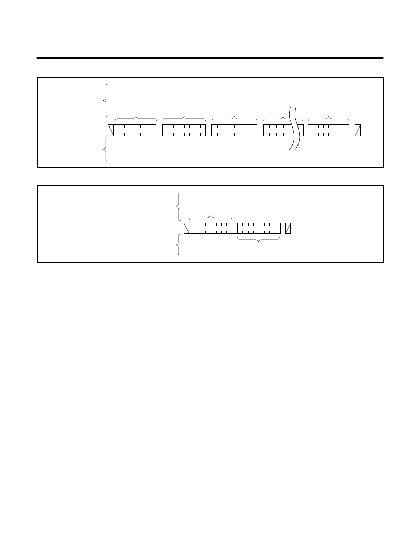
Figure 15. Page Write Sequence
Figure 16. Current Address Read Sequence
Word
Address 0
S
t
a
r
t
S
t
o
p
Slave
Address
Word
Address 1
Data
(n)
A
C
K
A
C
K
SDA Bus
Signals from
the Slave
Signals from
the Master
0
Data
(1)
(1
≤
n
≤
64)
1
1
1
1
0 0 0 0 0
A
C
K
A
C
K
S
t
a
r
t
S
t
o
p
Slave
Address
Data
A
C
K
SDA Bus
Signals from
the Slave
Signals from
the Master
1
1
1
1
1
Acknowledge Polling
Disabling of the inputs during nonvolatile write cycles
can be used to take advantage of the typical 5ms write
cycle time. Once the stop condition is issued to indi-
cate the end of the master’s byte load operation, the
X1242 initiates the internal nonvolatile write cycle.
Acknowledge polling can begin immediately. To do
this, the master issues a start condition followed by the
Slave Address Byte for a write or read operation. If the
X1242 is still busy with the nonvolatile write cycle then
no ACK will be returned. When the X1242 has com-
pleted the write operation, an ACK is returned and the
host can proceed with the read or write operation.
Refer to the flow chart in Figure 17.
Read Operations
There are three basic read operations: Current
Address Read, Random Read, and Sequential Read.
Current Address Read
Internally the X1242 contains an address counter that
maintains the address of the last word read incre-
mented by one. Therefore, if the last read was to
address n, the next read operation would access data
from address n + 1. On power up, the sixteen bit
address is initialized to 0h. In this way, a current
address read immediately after the power on reset can
download the entire contents of memory starting at the
first location.Upon receipt of the Slave Address Byte
with the R/W bit set to one, the X1242 issues an
acknowledge, then transmits eight data bits. The mas-
ter terminates the read operation by not responding
with an acknowledge during the ninth clock and issu-
ing a stop condition. Refer to Figure 15 for the
address, acknowledge, and data transfer sequence.
相關(guān)PDF資料 |
PDF描述 |
|---|---|
| x1243(中文) | Real Time Clock/Calendar/Alarm with EEPROM(帶EEPROM的實時時鐘/日歷/鬧鐘) |
| X12xx-EVM(中文) | Xicor RTC X12xx-EVM User Guide(XICOR RTC X12xx-EVM評估板使用說明) |
| X187 | TEMPERATURSICHERUNG 187GRAD 5ST |
| X25 | 40V Single N-Channel HEXFET Power MOSFET in a D2-Pak package; A IRL1004S with Standard Packaging |
| X2001D-20 | NVRAM (EEPROM Based) |
相關(guān)代理商/技術(shù)參數(shù) |
參數(shù)描述 |
|---|---|
| X1242S8 | 制造商:未知廠家 制造商全稱:未知廠家 功能描述:IC-SMD-RTC WITH EEPROM |
| X1243 | 制造商:INTERSIL 制造商全稱:Intersil Corporation 功能描述:Real Time Clock/Calendar/Alarm with EEPROM |
| X1243S8 | 制造商:XICOR 制造商全稱:Xicor Inc. 功能描述:Real Time Clock/Calendar/Alarm with EEPROM |
| X1243S8I | 制造商:Intersil Corporation 功能描述: 制造商:XICOR 功能描述: |
| X1243V8 | 制造商:XICOR 制造商全稱:Xicor Inc. 功能描述:Real Time Clock/Calendar/Alarm with EEPROM |
發(fā)布緊急采購,3分鐘左右您將得到回復(fù)。