- 您現(xiàn)在的位置:買賣IC網(wǎng) > PDF目錄140344 > WV3EG32M64ETSU335D3MG (MICROSEMI CORP-PMG MICROELECTRONICS) 32M X 64 DDR DRAM MODULE, 0.7 ns, DMA184 PDF資料下載
參數(shù)資料
| 型號(hào): | WV3EG32M64ETSU335D3MG |
| 廠商: | MICROSEMI CORP-PMG MICROELECTRONICS |
| 元件分類: | DRAM |
| 英文描述: | 32M X 64 DDR DRAM MODULE, 0.7 ns, DMA184 |
| 封裝: | ROHS COMPLIANT, DIMM-184 |
| 文件頁(yè)數(shù): | 10/12頁(yè) |
| 文件大小: | 247K |
| 代理商: | WV3EG32M64ETSU335D3MG |
White Electronic Designs
7
White Electronic Designs Corporation (602) 437-1520 www.whiteedc.com
July 2005
Rev. 0
ADVANCED
WV3EG32M64ETSU-D3
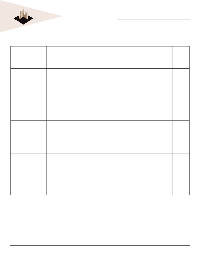
IDD SPECIFICATIONS AND TEST CONDITIONS
0°C TA 70°C, VCC = VCCQ = 2.5V ± 0.2V
Includes DDR SDRAM component only
Parameter
Symbol
Conditions
DDR333@
CL = 2.5
Units
Operating one bank active-
precharge current;
IDD0*
tCK = tCK(IDD), tRC = tRC(IDD), tRAS = tRASmin(IDD); CKE is HIGH, CS is HIGH
between valid commands; Address bus inputs are SWITCHING; Data bus inputs
are SWITCHING
720
mA
Operating one bank active-
read-precharge current;
IDD1*
IOUT = 0mA; BL = 4, CL = CL(IDD), AL = 0; tCK = tCK(IDD), tRC = tRC (IDD), tRAS =
tRASmin(IDD), tRCD = tRCD(IDD); CKE is HIGH, CS is HIGH between valid commands;
Address businputs are SWITCHING; Data pattern is same as IDD4W
920
mA
Precharge power-down
current;
IDD2P**
All banks idle; tCK = tCK(IDD); CKE is LOW; Other control and address bus inputs
are STABLE; Data bus inputs are FLOATING
24
mA
Precharge quiet standby
current;
IDD2F**
All banks idle; tCK = tCK(IDD); CKE is HIGH, CS is HIGH; Other control and address
bus inputs are STABLE; Data bus inputs are FLOATING
240
mA
Active power-down current;
IDD3P**
All banks open; tCK = tCK(IDD); CKE is LOW; Other control and address bus inputs
are STABLE; Data bus inputs are FLOATING
280
mA
Active standby current;
IDD3N**
All banks open; tCK = tCK(IDD), tRAS = tRASmax(IDD), tRP = tRP(IDD); CKE is HIGH,
CS - is HIGH between valid commands; Other control and address bus inputs are
SWITCHING; Data bus inputs are SWITCHING
440
mA
Operating burst read current;
IDD4R*
All banks open, Continuous burst reads, IOUT = 0mA; BL = 4, CL = CL(IDD), AL
= 0; tCK = tCK(IDD), tRAS = tRASmax(IDD), tRP = tRP(IDD); CKE is HIGH, CS is HIGH
between valid commands; Address bus inputs are SWITCHING; Data pattern is
same as IDD4W
1280
mA
Operating burst write current;
IDD4W*
All banks open, Continuous burst writes; BL = 4, CL = CL(IDD), AL = 0; tCK =
tCK(IDD), tRAS = tRAS-max(IDD), tRP = tRP(IDD); CKE is HIGH, CS is HIGH between
valid commands; Address bus inputs are SWITCHING; Data bus inputs are
SWITCHING
1280
mA
Burst auto refresh current;
IDD5**
tCK = tCK(IDD); Refresh command at every tRFC(IDD) interval; CKE is HIGH, CS
is HIGH between valid commands; Other control and address bus inputs are
SWITCHING; Data bus inputs are SWITCHING
1360
mA
Self refresh current;
IDD6**
CK and CK at 0V; CKE 0.2V; Other control and address bus inputs are
FLOATING; Data bus inputs are FLOATING
24
mA
Operating bank interleave
read current;
IDD7*
All bank interleaving reads, IOUT = 0mA; BL = 4, CL = CL(IDD), AL = tRCD(IDD)-
1*tCK(IDD); tCK = tCK(IDD), tRC = tRC(IDD), tRRD = tRRD(IDD), tRCD = 1*tCK(IDD); CKE is
HIGH, CS is HIGH between valid commands; Address bus inputs are STABLE
during DESELECTs; Data pattern is same as IDD4R; Refer to the following page for
detailed timing conditions
2240
mA
Note: These specications apply to modules built with Inneon components only.
* Value calculated as one module rank in this operation condition and other module rank in IDD2P (CKE low) mode.
** Value calculated as all module ranks in this operation condition.
相關(guān)PDF資料 |
PDF描述 |
|---|---|
| WF512K32-90G1UQ5 | 512K X 32 FLASH 5V PROM MODULE, 90 ns, CQFP68 |
| WED3EL7216S7BC | 16M X 72 DDR DRAM, 0.75 ns, PBGA219 |
| WS128K32L-25G1TC | 128K X 32 MULTI DEVICE SRAM MODULE, 25 ns, CQFP68 |
| WS128K32L-35G1TC | 128K X 32 MULTI DEVICE SRAM MODULE, 35 ns, CQFP68 |
| W3EG64129S262D3 | 128M X 64 DDR DRAM MODULE, DMA184 |
相關(guān)代理商/技術(shù)參數(shù) |
參數(shù)描述 |
|---|---|
| WV3EG32M64ETSU335D3SG | 制造商:WEDC 制造商全稱:White Electronic Designs Corporation 功能描述:256MB - 32Mx64 DDR SDRAM UNBUFFERED |
| WV3EG32M64ETSU-D3 | 制造商:WEDC 制造商全稱:White Electronic Designs Corporation 功能描述:256MB - 32Mx64 DDR SDRAM UNBUFFERED |
| WV3EG6434S262BD4 | 制造商:WEDC 制造商全稱:White Electronic Designs Corporation 功能描述:256MB - 32Mx64 DDR SDRAM UNBUFFERED, w/PLL |
| WV3EG6434S265BD4 | 制造商:WEDC 制造商全稱:White Electronic Designs Corporation 功能描述:256MB - 32Mx64 DDR SDRAM UNBUFFERED, w/PLL |
| WV3EG6434S335BD4 | 制造商:WEDC 制造商全稱:White Electronic Designs Corporation 功能描述:256MB - 32Mx64 DDR SDRAM UNBUFFERED, w/PLL |
發(fā)布緊急采購(gòu),3分鐘左右您將得到回復(fù)。