- 您現(xiàn)在的位置:買賣IC網(wǎng) > PDF目錄361880 > WM8148 (Wolfson Microelectronics) TVS BIDIRECT 400W 5.0V SMA PDF資料下載
參數(shù)資料
| 型號: | WM8148 |
| 廠商: | Wolfson Microelectronics |
| 英文描述: | TVS BIDIRECT 400W 5.0V SMA |
| 中文描述: | 12-bit/12MSPS防治荒漠化公約/獨聯(lián)體模擬前端/數(shù)字轉(zhuǎn)換器 |
| 文件頁數(shù): | 15/43頁 |
| 文件大?。?/td> | 491K |
| 代理商: | WM8148 |
第1頁第2頁第3頁第4頁第5頁第6頁第7頁第8頁第9頁第10頁第11頁第12頁第13頁第14頁當前第15頁第16頁第17頁第18頁第19頁第20頁第21頁第22頁第23頁第24頁第25頁第26頁第27頁第28頁第29頁第30頁第31頁第32頁第33頁第34頁第35頁第36頁第37頁第38頁第39頁第40頁第41頁第42頁第43頁
WM8148
Production Data
WOLFSON MICROELECTRONICS LTD
PD Rev 4.0 April 1999
15
DEVICE DESCRIPTION
INTRODUCTION
The WM8148 samples up to three analogue inputs simultaneously, conditions these signals and
converts each resulting analogue signal to a 12-bit digital word.
A block diagram is shown on page 1. Each of the three input channels consists of an Input Sampling
block (CDS/RLC), an 8-bit programmable Offset DAC, and a 6-bit Programmable Gain Amplifier
(PGA). The outputs from the three channels are multiplexed into a 12-bit ADC. The digital output from
the ADC is presented on a 12-bit wide bi-directional bus.
A high-speed (up to 48MHz) master clock, MCLK, and a per-pixel synchronisation pulse, VSMP, drive
a shared Timing Control block to generate input sampling signals and other internal clocks.
Alternatively the device can operate from MCLK only, outputting VSMP synchronisation pulses to the
rest of the system.
An internal reference provides buffered voltages VRT, VRB and VRX. A 4-bit DAC (RLC DAC)
provides a programmable buffered voltage at pin VRLC for use as an input signal reference level or
an input clamp voltage.
The operation of the device is controlled by internal control registers, which can be read from and
written to via a Digital Management Interface (DMI) in either serial or parallel mode.
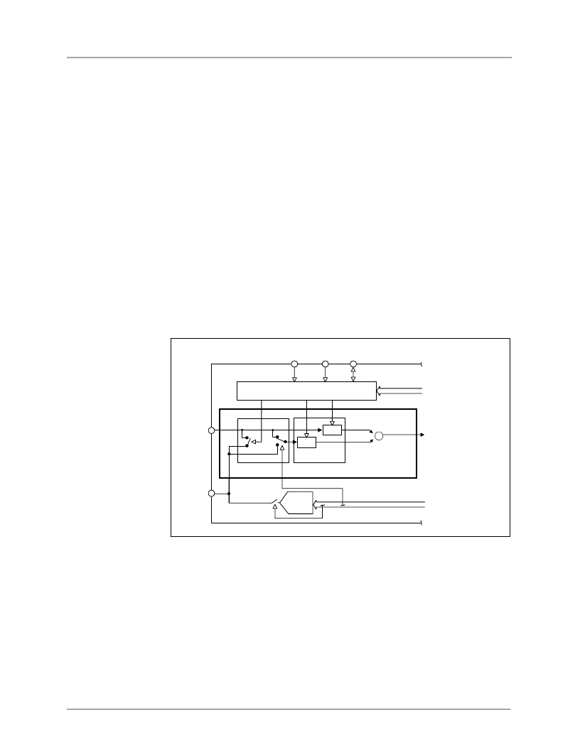
INPUT SAMPLING
Figure 14 shows the configuration of the Input Sampling Block for the red channel. (The green and
blue channels are the same.)
TIMING CONTROL
R
S
RINP
VRLC
S/H
4-BIT
RLC DAC
CL
+
+
-
To Offset DAC
RLC
CDS
From Control Interface
S/H
V
S
From Control Interface
MCLK
VSMP
RLC
INPUT SAMPLING
BLOCK FOR RED
CHANNEL
MODE[0]
Figure 14 Input Sampling Block – Configuration for Red Channel
This block contains switches to perform Reset Level Clamping (RLC) and Correlated Double
Sampling (CDS). Sample/Hold blocks sample the video and reset/reference levels of the input
waveform, and pass the difference signal on to the rest of the channel. Internal clocks V
S
and R
S
define the timing of the sampling of the video signal and the reset/reference level respectively. When
enabled by control input pin RLC, internal signal CL clamps the input pin RINP to the voltage on pin
VRLC, which is driven either externally or from the 4-bit RLC DAC.
The detailed timing of the internal clock signals CL, V
S
, and R
S,
with respect to VSMP and MCLK, is
controlled by the Timing Control block as programmed via the Digital Management Interface (DMI).
相關(guān)PDF資料 |
PDF描述 |
|---|---|
| WM8150 | DIODE TVS 400W 5V UNI DIR |
| WM8150CDS | SINGLE CHANNEL 12 BIT CIS/CCD AFE WITH 4 BIT WIDE OUTPUT |
| WM8150CDSR | SINGLE CHANNEL 12 BIT CIS/CCD AFE WITH 4 BIT WIDE OUTPUT |
| WM8170 | 5.0 VOLT BI-DIRECTIONAL TRANSIENT VOLTAGE SUPPRESSOR |
| WM8181 | 12-bit 2MSPS Serial Output CIS/CCD Digitiser |
相關(guān)代理商/技術(shù)參數(shù) |
參數(shù)描述 |
|---|---|
| WM8150 | 制造商:WOLFSON 制造商全稱:WOLFSON 功能描述:SINGLE CHANNEL 12 BIT CIS/CCD AFE WITH 4 BIT WIDE OUTPUT |
| WM8150_05 | 制造商:WOLFSON 制造商全稱:WOLFSON 功能描述:Single Channel 12-bit CIS/CCD AFE with 4-bit Wide Output |
| WM8150CDS | 制造商:WOLFSON 制造商全稱:WOLFSON 功能描述:SINGLE CHANNEL 12 BIT CIS/CCD AFE WITH 4 BIT WIDE OUTPUT |
| WM8150CDS/R | 制造商:WOLFSON 制造商全稱:WOLFSON 功能描述:Single Channel 12-bit CIS/CCD AFE with 4-bit Wide Output |
| WM8150CDSR | 制造商:WOLFSON 制造商全稱:WOLFSON 功能描述:SINGLE CHANNEL 12 BIT CIS/CCD AFE WITH 4 BIT WIDE OUTPUT |
發(fā)布緊急采購,3分鐘左右您將得到回復。