- 您現(xiàn)在的位置:買賣IC網(wǎng) > PDF目錄140343 > WED2DL36514V25BC (WHITE ELECTRONIC DESIGNS CORP) 512K X 36 STANDARD SRAM, 2.5 ns, PBGA119 PDF資料下載
參數(shù)資料
| 型號(hào): | WED2DL36514V25BC |
| 廠商: | WHITE ELECTRONIC DESIGNS CORP |
| 元件分類: | SRAM |
| 英文描述: | 512K X 36 STANDARD SRAM, 2.5 ns, PBGA119 |
| 封裝: | PLASTIC, BGA-119 |
| 文件頁(yè)數(shù): | 7/12頁(yè) |
| 文件大小: | 266K |
| 代理商: | WED2DL36514V25BC |
4
White Electronic Designs Corporation (508) 366-5151 www.whiteedc.com
WED2DL36513V
WED2DL36513AV
ABSOLUTE MAXIMUM RATINGS*
Voltage on VDD Supply relative to VSS
-0.5V to +4.6V
Voltage on VDDQ Supply relative to VSS
-0.5V to +4.6V
VIN (DQx)
-0.5V to VDDQ +0.5V
VIN (Inputs)
-0.5V to VDD +0.5V
Storage Temperature (BGA)
+55
°C to +125°C
Short Circuit Output Current
100 mA
*Stress greater than those listed under "Absolute Maximum Ratings" may cause
permanent damage to the device. This is a stress rating only and functional operation
of the device at these or any other conditions greater than those indicated in the
operational sections of this specification is not implied. Exposure to absolute maximum
rating conditions for extended periods may affect reliability.
ELECTRICAL CHARACTERISTICS
Description
Symbol
Conditions
Min
Max
Units
Notes
Input High (Logic 1)Voltage
VIH
2.0
VDD +0.3
V
1
Input Low (Logic 0) Voltage
VIL
-0.3
0.8
V
1
Input Leakage Current
ILI
0V
≤ VIN ≤ VDD
-1.0
1.0
mA
2
Ouptut Leakage Current
ILO
Output(s) disabled, 0V
≤ VIN ≤ VDD
-1.0
1.0
mA
Output High Voltage
VOH
IOH = -4.0mA
2.4
—
V
1
Output Low Voltage
VOL
IOL = 8.0mA
—
0.4
V
1
Supply Voltage
VDD
3.135
3.6
V
1
Isolated Output Buffer Supply
VDDQ
3.134
3.6
V
NOTES:
1. All voltages referenced to Vss (GND).
2. MODE has an internal pull-up, and input leakage =
±10liA.
Description
Conditions
Symbol
Typ
Max
Units
Notes
Control Input Capacitance
TA = 25
°C; f = 1MHz
CI
34
pF
1
Input/Output Capacitance (DQ)
TA = 25
°C; f = 1MHz
CO
45
pF
1
Address Capacitance
TA = 25
°C; f = 1MHz
CA
35
pF
1
Clock Capacitance
TA = 25
°C; f = 1MHz
CCK
2.5
4
pF
1
NOTES:
1. This parameter is sampled.
BGA CAPACITANCE
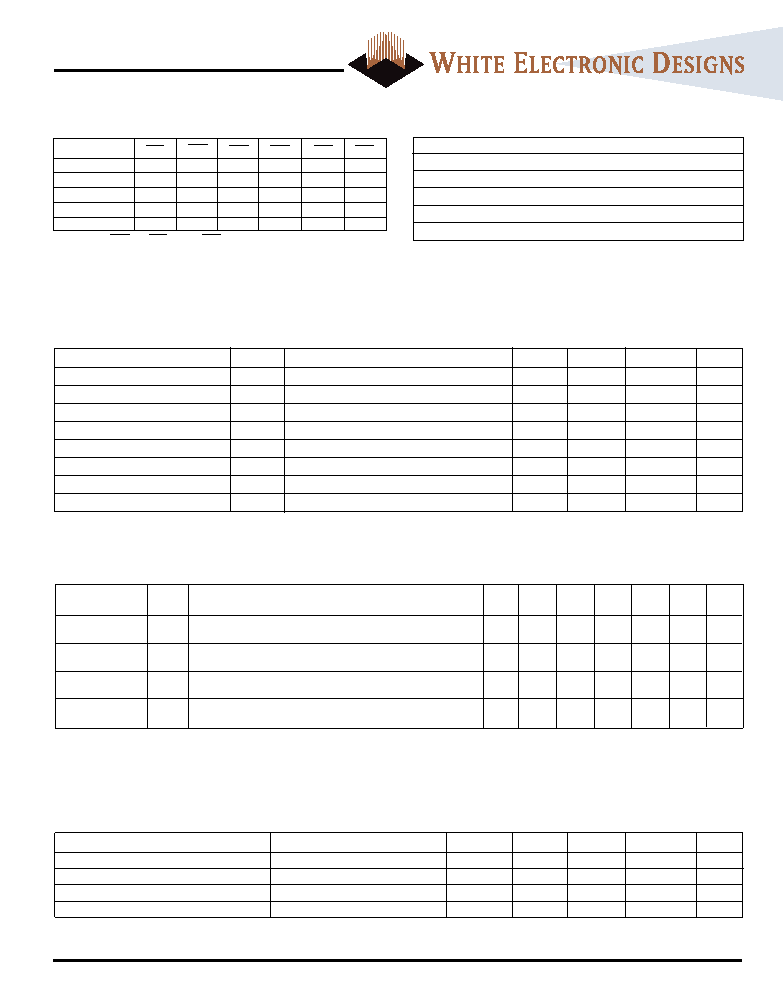
PARTIAL TRUTH TABLE - WRITE COMMANDS
Function
GW
BWE
BWa
BWb
BWc
BWd
Read
H
X
Read
H
L
H
Write Byte “a”
H
L
H
Write All Bytes
H
L
Write All Bytes
L
X
NOTE: Using BWE and BWa through BWd, any one or more bytes may be written.
Description
Symbol
Conditions
Typ
200*
166
150
133
Units
Notes
MHz
Power Supply
Device selected; All inputs
≤ VIL or 3 VIH; Cycle time 3 tKC MIN;
Current: Operating
IDD
VDD = MAX; Outputs open
TBD
700
620
560
mA
1,2,3
Device deselected; VDD = MAX; All inputs
≤ VSS + 0.2
CMOS Standby
ISB2
or VDD - 0.2; All inputs static; CLK frequency = 0
10
20
mA
2,3
Device deselected; VDD = MAX; All inputs
≤ VIL or VIH;
TTL Standby
ISB3
All inputs static; CLD frequency = 0
20
40
mA
2,3
Device deselected; VDD = MAX; All inputs
≤ VSS + 0.2
Clock Running
ISB4
or VDD -0.2; Cycle time 3 tKC MIN
80
TBD
180
160
140
mA
2,3
* Advanced Information
NOTES:
1. IDD is specified with no output current and increases with faster cycle times. IDD increases with faster cycle times and greater output loading.
2. “Device deselected” means device is in power-down mode as defined in the truth table. “Device selected” means device is active (not in power-down mode).
3. Typical values are measured at 3.3V, 250
°C and 10ns cycle time.
DC CHARACTERISTICS
相關(guān)PDF資料 |
PDF描述 |
|---|---|
| WED7F2325ZXEBSN70C | 1M X 32 FLASH 5V PROM MODULE, 70 ns, SMA80 |
| WS128K32-25G4TME | 512K X 8 MULTI DEVICE SRAM MODULE, 25 ns, CQFP68 |
| WS128K32N-35HQE | 512K X 8 MULTI DEVICE SRAM MODULE, 35 ns, CPGA66 |
| WS256K32N-25HCA | 256K X 32 MULTI DEVICE SRAM MODULE, 25 ns, CPGA66 |
| WS256K32N-35G4I | 256K X 32 MULTI DEVICE SRAM MODULE, 35 ns, CQFP68 |
相關(guān)代理商/技術(shù)參數(shù) |
參數(shù)描述 |
|---|---|
| WED2EG472512V5D2 | 制造商:WEDC 制造商全稱:White Electronic Designs Corporation 功能描述:16MB (4x512Kx72) SYNC BURST PIPELINE, DUAL KEY DIMM |
| WED2EG472512V65D2 | 制造商:WEDC 制造商全稱:White Electronic Designs Corporation 功能描述:16MB (4x512Kx72) SYNC BURST PIPELINE, DUAL KEY DIMM |
| WED2EG472512V6D2 | 制造商:WEDC 制造商全稱:White Electronic Designs Corporation 功能描述:16MB (4x512Kx72) SYNC BURST PIPELINE, DUAL KEY DIMM |
| WED2EG472512V7D2 | 制造商:WEDC 制造商全稱:White Electronic Designs Corporation 功能描述:16MB (4x512Kx72) SYNC BURST PIPELINE, DUAL KEY DIMM |
| WED2EG472512V-D2 | 制造商:WEDC 制造商全稱:White Electronic Designs Corporation 功能描述:16MB (4x512Kx72) SYNC BURST PIPELINE, DUAL KEY DIMM |
發(fā)布緊急采購(gòu),3分鐘左右您將得到回復(fù)。