- 您現(xiàn)在的位置:買賣IC網(wǎng) > PDF目錄140343 > WED2DL36514V25BC (WHITE ELECTRONIC DESIGNS CORP) 512K X 36 STANDARD SRAM, 2.5 ns, PBGA119 PDF資料下載
參數(shù)資料
| 型號(hào): | WED2DL36514V25BC |
| 廠商: | WHITE ELECTRONIC DESIGNS CORP |
| 元件分類: | SRAM |
| 英文描述: | 512K X 36 STANDARD SRAM, 2.5 ns, PBGA119 |
| 封裝: | PLASTIC, BGA-119 |
| 文件頁(yè)數(shù): | 6/12頁(yè) |
| 文件大小: | 266K |
| 代理商: | WED2DL36514V25BC |
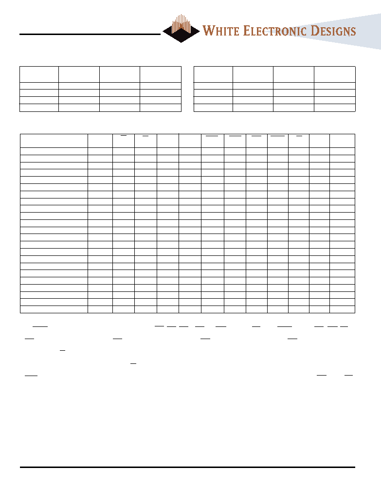
3
White Electronic Designs Corporation (508) 366-5151 www.whiteedc.com
WED2DL36513V
WED2DL36513AV
INTERLEAVED BURST TABLE (MODE = NC OR HIGH)
First Address
Second Address
Third Address
Fourth Address
External
Internal
X...X00
X...X01
X...X10
X...X11
X...X01
X....X00
X...X11
X...X10
X...X11
X...X00
X...X01
X...X11
X...X10
X...X01
X...X00
INTERLEAVED BURST TABLE (MODE = LOW)
First Address
Second Address
Third Address
Fourth Address
External
Internal
X...X00
X...X01
X...X10
X...X11
X...X01
X....X10
X...X11
X...X00
X...X10
X...X11
X...X00
X...X01
X...X11
X...X00
X...X01
X...X10
TRUTH TABLE
Function
Address
CE
CE2
ZZ
ADSP
ADSC
ADV
WRITE
OE
CLK
DQ
Used
Deselected Cycle,Power-Down
None
H
X
L
X
L
X
L-H
High-Z
Deselected Cycle,Power-Down
None
L
X
L
X
L-H
High-Z
Deselected Cycle,Power-Down
None
L
H
X
L
X
L-H
High-Z
Deselected Cycle,Power-Down
None
L
X
L
H
L
X
L-H
High-Z
Deselected Cycle,Power-Down
None
L
H
X
L
H
L
X
L-H
High-Z
SNOOZE MODE,Power-Down
None
X
H
X
High-Z
READ Cycle, Begin Burst
External
L
H
L
X
L
L-H
Q
READ Cycle, Begin Burst
External
L
H
L
X
H
L-H
High-Z
WRITE Cycle Begin Burst
External
L
H
L
H
L
X
L
X
L-H
D
READ Cycle Begin Burst
External
L
H
L
H
L
X
H
L
L-H
Q
READ Cycle Begin Burst
External
L
H
L
H
L
X
H
L-H
High-Z
READ Cycle, Continue Burst
Next
X
L
H
L
H
L
L-H
Q
READ Cycle, Continue Burst
Next
X
L
H
L
H
L-H
High-Z
READ Cycle, Continue Burst
Next
H
X
L
X
H
L
H
L
L-H
Q
READ Cycle, Continue Burst
Next
H
X
L
X
H
L
H
L-H
High-Z
WRITE Cycle, Continue Burst
Next
X
L
H
L
X
L-H
D
WRITE Cycle, Continue Burst
Next
H
X
L
X
H
L
X
L-H
D
READ Cycle, Suspend Burst
Current
X
L
H
L
L-H
Q
READ Cycle, Suspend Burst
Current
X
L
H
HHHH
L-H
High-Z
READ Cycle, Suspend Burst
Current
H
X
L
X
H
L
L-H
Q
READ Cycle, Suspend Burst
Current
H
X
L
X
HHHH
L-H
High-Z
WRITE Cycle, Suspend Burst
Current
X
L
H
L
X
L-H
D
WRITE Cycle, Suspend Burst
Current
H
X
L
X
H
L
X
L-H
D
NOTES:
1. X means “Don’t Care.” —— means active LOW. H means logic HIGH. L means logic LOW.
2. For WRITE, L means any one or more byte write enable signals (BWa, BWb, BWc or BWd) and BWE are LOW or GW is LOW. WRITE = H for all BWx, BWE, GW
HIGH.
3. BWa enables WRITEs to DQa’s and DQPa. BWb enables WRITEs to DQb’s and DQPb. BWc enables WRITEs to DQc’s and DQPc. BWd enables WRITEs to DQd’s
and DQPd.
4. All inputs except OE and ZZ must meet setup and hold times around the rising edge (LOW to HIGH) of CLK.
5. Wait states are inserted by suspending burst.
6. For a WRITE operation following a READ operation, OE must be HIGH before the input data setup time and held HIGH throughout the input data hold time.
7. This device contains circuitry that will ensure the outputs will be in High-Z during power-up.
8. ADSP LOW always initiates an internal READ at the L-H edge of CLK A WRITE is performed by setting one or more byte write enable signals and BWE LOW or GW
LOW for the subsequent L-H edge of CLK. Refer to WRITE timing diagram for clarification.
相關(guān)PDF資料 |
PDF描述 |
|---|---|
| WED7F2325ZXEBSN70C | 1M X 32 FLASH 5V PROM MODULE, 70 ns, SMA80 |
| WS128K32-25G4TME | 512K X 8 MULTI DEVICE SRAM MODULE, 25 ns, CQFP68 |
| WS128K32N-35HQE | 512K X 8 MULTI DEVICE SRAM MODULE, 35 ns, CPGA66 |
| WS256K32N-25HCA | 256K X 32 MULTI DEVICE SRAM MODULE, 25 ns, CPGA66 |
| WS256K32N-35G4I | 256K X 32 MULTI DEVICE SRAM MODULE, 35 ns, CQFP68 |
相關(guān)代理商/技術(shù)參數(shù) |
參數(shù)描述 |
|---|---|
| WED2EG472512V5D2 | 制造商:WEDC 制造商全稱:White Electronic Designs Corporation 功能描述:16MB (4x512Kx72) SYNC BURST PIPELINE, DUAL KEY DIMM |
| WED2EG472512V65D2 | 制造商:WEDC 制造商全稱:White Electronic Designs Corporation 功能描述:16MB (4x512Kx72) SYNC BURST PIPELINE, DUAL KEY DIMM |
| WED2EG472512V6D2 | 制造商:WEDC 制造商全稱:White Electronic Designs Corporation 功能描述:16MB (4x512Kx72) SYNC BURST PIPELINE, DUAL KEY DIMM |
| WED2EG472512V7D2 | 制造商:WEDC 制造商全稱:White Electronic Designs Corporation 功能描述:16MB (4x512Kx72) SYNC BURST PIPELINE, DUAL KEY DIMM |
| WED2EG472512V-D2 | 制造商:WEDC 制造商全稱:White Electronic Designs Corporation 功能描述:16MB (4x512Kx72) SYNC BURST PIPELINE, DUAL KEY DIMM |
發(fā)布緊急采購(gòu),3分鐘左右您將得到回復(fù)。