- 您現(xiàn)在的位置:買賣IC網(wǎng) > PDF目錄140343 > WED2DL36514V25BC (WHITE ELECTRONIC DESIGNS CORP) 512K X 36 STANDARD SRAM, 2.5 ns, PBGA119 PDF資料下載
參數(shù)資料
| 型號: | WED2DL36514V25BC |
| 廠商: | WHITE ELECTRONIC DESIGNS CORP |
| 元件分類: | SRAM |
| 英文描述: | 512K X 36 STANDARD SRAM, 2.5 ns, PBGA119 |
| 封裝: | PLASTIC, BGA-119 |
| 文件頁數(shù): | 5/12頁 |
| 文件大小: | 266K |
| 代理商: | WED2DL36514V25BC |
2
White Electronic Designs Corporation (508) 366-5151 www.whiteedc.com
WED2DL36513V
WED2DL36513AV
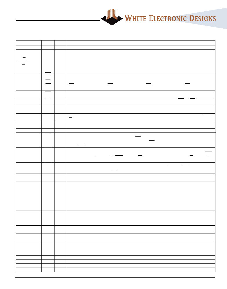
PIN DESCRIPTION
x36
Symbol
Type
Description
CLK
Input
Pulse
The system clock input. All of the SSRAM inputs are sampled on the rising edge of the clock.
4P
SA0
Input
Synchronous Address Inputs: These inputs are registered and must meet the setup and hold times around the rising edge of
4N
SA1
CLK.
2A, 2C, 2R, 2B
SA
3A, 3B, 3C, 3T
4T, 5A, 5B, 5C,
5T, 6A, 6B, 6C, 6R
5L
BWa
Input
Synchronous Byte Write Enables: These active LOW inputs allow individual bytes to be written and must meet the setup
5G
BWb
and hold times around the rising edge of CLK. A byte write enable is LOW for a WRITE cycle and HIGH for a READ cycle.
3G
BWc
3L
BWd
BWa controls DQa’s and DQPa; BWb controls DQb’s and DQPb; BWc controls DQc’s and DQPc; BWd controls DQd’s and
DQPd.
4M
BWE
Input
Byte Write Enable: This active LOW input permits BYTE WRITE operations and must meet the setup and hold times
around the rising edge of CLK.
4H
GW
Input
Global Write: This active LOW input allows a full 36- bit WRITE to occur independent of the BWE and BWx lines and must
meet the setup and hold times around the rising edge of CLK.
4K
CLK
Input
Clock: This signal registers the address, data, chip enable, byte write enables and burst control inputs on its rising edge.
All synchronous inputs must meet setup and hold times around the clock’s rising edge.
4E
CE
Input
Synchronous Chip Enable: This active LOW input is used to enable the device and conditions the internal use of ADSP.
CE is sampled only when a new external address is loaded.
7T
ZZ
Input
Snooze Enable: This active HIGH, asynchronous input causes the device to enter a low-power standby mode in which all
data in the memory array is retained. When active, all other inputs are ignored.
4F
OE
Input
Output Enable: This active LOW, asynchronous input enables the data I/O output drivers.
4G
ADV
Input
Synchronous Address Advance: This active LOW input is used to advance the internal burst counter, controlling burst
access after the external address is loaded. A HIGH on ADV effectively causes wait states to be generated (no address
advance). To ensure use of correct address during a WRITE cycle, ADV must be HIGH at the rising edge of the first clock
after an ADSP cycle is initiated.
4A
ADSP
Input
Synchronous Address Status Processor: This active LOW input interrupts any ongoing burst, causing a new external
address to be registered. A READ is performed using the new address, independent of the byte write enables and ADSC,
but dependent upon CE, CE2 and CE2. ADSP is ignored if CE is HIGH. Powerdown state is entered if CE2 is LOW or CE2
is HIGH .
4B
ADSC
Input
Synchronous Address Status Controller: This active LOW input interrupts any ongoing burst, causing a new external
address to be registered. A READ or WRITE is performed using the new address if CE is LOW. ADSC is also used to place
the chip into power-down state when CE is HIGH.
3R
MODE
Input
Mode: This input selects the burst sequence. A LOW on MODE selects “l(fā)inear burst.” NC or HIGH on this input selects
“interleaved burst.” Do not alter input state while device is operating.
(a) 6K, 6L, 6M, 6N,
DQa
Input/
SRAM Data I/Os: Byte “a” is DQa’s; Byte “b” is DQb’s; Byte “c” is DQc’s;
7K, 7L, 7N, 7P
Output
Byte “d” is DQd’s. Input data must meet setup and hold times around rising edge of CLK.
(b) 6E, 6F, 6G, 6H,
DQb
7D, 7E, 7G, 7H
(c) 1D, 1E, 1G, 1H
DQc
2E, 2F, 2G, 2H
(d) 1K, 1L, 1N, 1P,
DQd
2K, 2L, 2M, 2N
6P
DQPa
Input/
Byte “a” Parity is DQPa; Byte “b” Parity is DQPb; Byte “c” Parity is DQPc;
6D
DQPb
Output
Byte “d” Parity is DQPd.
2D
DQPc
2P
DQPd
2J, 4C, 4J, 4R, 5R,
VDD
Supply
Power Supply: See DC Electrical Characteristics and Operating Conditions for range.
6J
1A, 1F, 1J, 1M 1U
VDDQ
Supply
Isolated Output Buffer Supply: See DC Electrical Characteristics and Operating
7A, 7F, 7J, 7M, 7U
Conditions for range.
3D, 3E, 3F, 3H, 3K,
VSS
Supply
Ground: GND.
3M, 3N, 3P, 5D, 5E,
5F, 5H, 5K, 5M, 5N,
5P
2U
TMS
Input
Scan Test Mode Select
3U
TDI
Input
Scan Test Data In
4U
TDO
Output
Scan Test Data Out
5U
TCK
Input
Scan Test Clock
相關(guān)PDF資料 |
PDF描述 |
|---|---|
| WED7F2325ZXEBSN70C | 1M X 32 FLASH 5V PROM MODULE, 70 ns, SMA80 |
| WS128K32-25G4TME | 512K X 8 MULTI DEVICE SRAM MODULE, 25 ns, CQFP68 |
| WS128K32N-35HQE | 512K X 8 MULTI DEVICE SRAM MODULE, 35 ns, CPGA66 |
| WS256K32N-25HCA | 256K X 32 MULTI DEVICE SRAM MODULE, 25 ns, CPGA66 |
| WS256K32N-35G4I | 256K X 32 MULTI DEVICE SRAM MODULE, 35 ns, CQFP68 |
相關(guān)代理商/技術(shù)參數(shù) |
參數(shù)描述 |
|---|---|
| WED2EG472512V5D2 | 制造商:WEDC 制造商全稱:White Electronic Designs Corporation 功能描述:16MB (4x512Kx72) SYNC BURST PIPELINE, DUAL KEY DIMM |
| WED2EG472512V65D2 | 制造商:WEDC 制造商全稱:White Electronic Designs Corporation 功能描述:16MB (4x512Kx72) SYNC BURST PIPELINE, DUAL KEY DIMM |
| WED2EG472512V6D2 | 制造商:WEDC 制造商全稱:White Electronic Designs Corporation 功能描述:16MB (4x512Kx72) SYNC BURST PIPELINE, DUAL KEY DIMM |
| WED2EG472512V7D2 | 制造商:WEDC 制造商全稱:White Electronic Designs Corporation 功能描述:16MB (4x512Kx72) SYNC BURST PIPELINE, DUAL KEY DIMM |
| WED2EG472512V-D2 | 制造商:WEDC 制造商全稱:White Electronic Designs Corporation 功能描述:16MB (4x512Kx72) SYNC BURST PIPELINE, DUAL KEY DIMM |
發(fā)布緊急采購,3分鐘左右您將得到回復(fù)。