- 您現(xiàn)在的位置:買(mǎi)賣(mài)IC網(wǎng) > PDF目錄202140 > W949D2CBJX5E (WINBOND ELECTRONICS CORP) 16M X 32 DDR DRAM, 5 ns, PBGA90 PDF資料下載
參數(shù)資料
| 型號(hào): | W949D2CBJX5E |
| 廠商: | WINBOND ELECTRONICS CORP |
| 元件分類(lèi): | DRAM |
| 英文描述: | 16M X 32 DDR DRAM, 5 ns, PBGA90 |
| 封裝: | 8 X 13 MM, 0.80 MM PITCH, HALOGEN FREE AND LEAD FREE, VFBGA-90 |
| 文件頁(yè)數(shù): | 43/60頁(yè) |
| 文件大?。?/td> | 1160K |
| 代理商: | W949D2CBJX5E |
第1頁(yè)第2頁(yè)第3頁(yè)第4頁(yè)第5頁(yè)第6頁(yè)第7頁(yè)第8頁(yè)第9頁(yè)第10頁(yè)第11頁(yè)第12頁(yè)第13頁(yè)第14頁(yè)第15頁(yè)第16頁(yè)第17頁(yè)第18頁(yè)第19頁(yè)第20頁(yè)第21頁(yè)第22頁(yè)第23頁(yè)第24頁(yè)第25頁(yè)第26頁(yè)第27頁(yè)第28頁(yè)第29頁(yè)第30頁(yè)第31頁(yè)第32頁(yè)第33頁(yè)第34頁(yè)第35頁(yè)第36頁(yè)第37頁(yè)第38頁(yè)第39頁(yè)第40頁(yè)第41頁(yè)第42頁(yè)當(dāng)前第43頁(yè)第44頁(yè)第45頁(yè)第46頁(yè)第47頁(yè)第48頁(yè)第49頁(yè)第50頁(yè)第51頁(yè)第52頁(yè)第53頁(yè)第54頁(yè)第55頁(yè)第56頁(yè)第57頁(yè)第58頁(yè)第59頁(yè)第60頁(yè)
W949D6CB / W949D2CB
512Mb Mobile LPDDR
Publication Release Date: Jun, 14, 2011
- 48 -
Revision A01-006
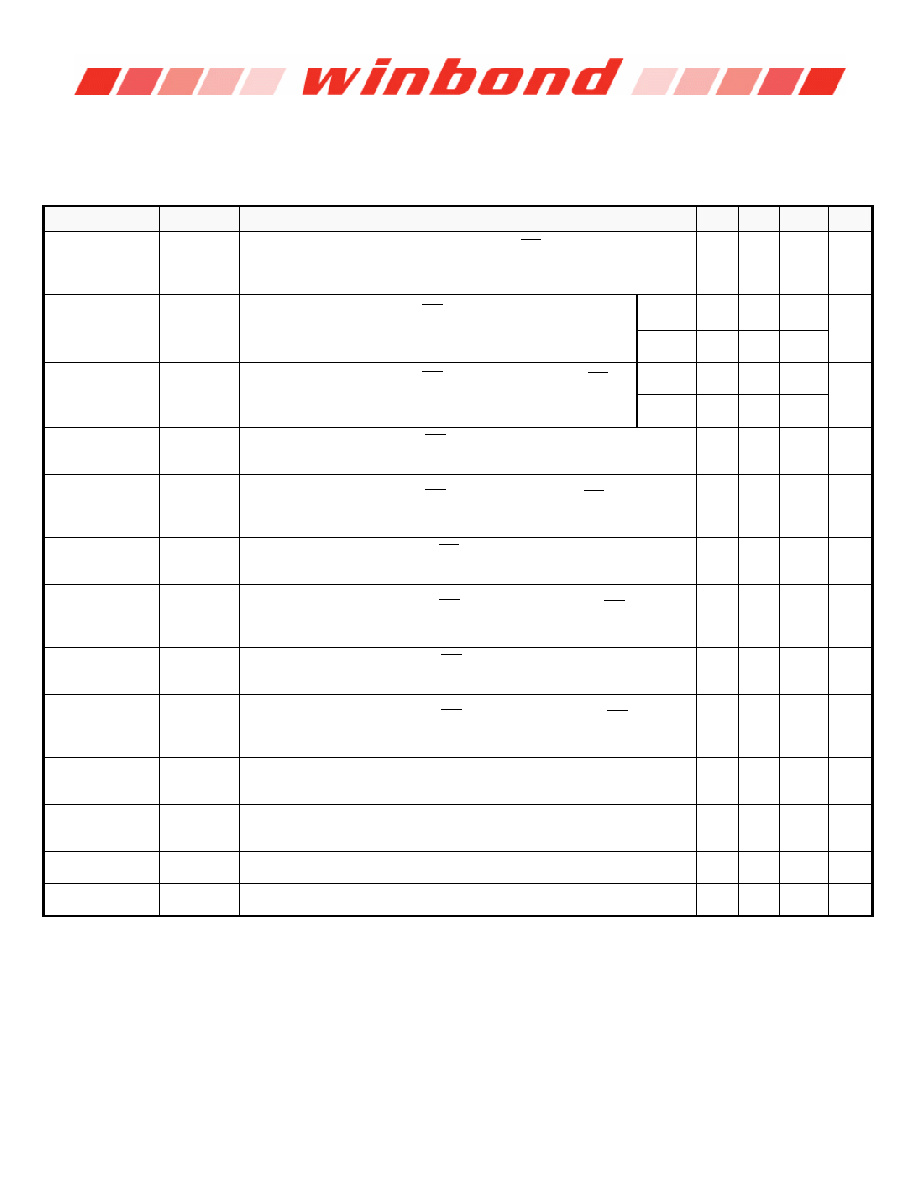
8.4 IDD Specification Parameters and Test Conditions
8.4.1 IDD Specification Parameters and Test Conditions
[Recommended Operating Conditions; Notes 1-4]
(512Mb, X16)
PARAMETER
SYMBOL
TEST CONDITION
- 5
- 6
- 75
UNIT
Operating one
bank active-
precharge
current
IDD0
tRC = tRCmin ; tCK = tCKmin ; CKE is HIGH;
CS is HIGH between valid
commands; address inputs are SWITCHING; data bus inputs are
STABLE
40
38
35
mA
Precharge
power-down
standby current
IDD2P
all banks idle, CKE is LOW;
CS is HIGH, tCK = tCKmin ;
address and control inputs are SWITCHING; data bus inputs
are STABLE
Low
power
0.6
mA
Normal
power
0.8
Precharge
power-down
standby current
with clock stop
IDD2PS
all banks idle, CKE is LOW;
CS is HIGH, CK = LOW,
=
HIGH; address and control inputs are SWITCHING; data bus
inputs are STABLE
Low
power
0.6
mA
Normal
power
0.8
Precharge non
power-down
standby current
IDD2N
all banks idle, CKE is HIGH;
CS is HIGH, tCK = tCKmin; address and
control inputs are SWITCHING; data bus inputs are STABLE
10
mA
Precharge non
power-down
standby current
with clock stop
IDD2NS
all banks idle, CKE is HIGH;
CS is HIGH, CK = LOW,
= HIGH;
address and control inputs are SWITCHING; data bus inputs are STABLE
3
mA
Active power-
down standby
current
IDD3P
one bank active, CKE is LOW;
CS is HIGH, tCK = tCKmin;address and
control inputs are SWITCHING; data bus inputs are STABLE
2
mA
Active power-
down standby
current with
clock stop
IDD3PS
one bank active, CKE is LOW;
CS is HIGH, CK = LOW,
= HIGH;
address and control inputs are SWITCHING; data bus inputs are STABLE
2
mA
Active non
power-down
standby current
IDD3N
one bank active, CKE is HIGH;
CS is HIGH, tCK = tCKmin; address
and control inputs are SWITCHING; data bus inputs are STABLE
15
mA
Active non
power-down
standby current
with clock stop
IDD3NS
one bank active, CKE is HIGH;
CS is HIGH, CK = LOW,
= HIGH;
address and control inputs are SWITCHING; data bus inputs are STABLE
8
mA
Operating burst
read current
IDD4R
one bank active; BL = 4; CL = 3; tCK = tCKmin ; continuous read bursts;
IOUT = 0 mA; address inputs are SWITCHING; 50% data change each
burst transfer
75
70
mA
Operating burst
write current
IDD4W
one bank active; BL = 4; t CK = t CKmin ; continuous write
bursts; address inputs are SWITCHING; 50% data change each burst
transfer
55
50
mA
Auto-Refresh
Current
IDD5
tRC = tRFCmin ; tCK = tCKmin ; burst refresh; CKE is HIGH; address and
control inputs are SWITCHING; data bus inputs are STABLE
75
mA
Deep Power-
Down current
IDD8(4)
Address and control inputs are STABLE; data bus inputs are STABLE
10
uA
CK
相關(guān)PDF資料 |
PDF描述 |
|---|---|
| WF128K32N-150HC5 | 512K X 8 FLASH 5V PROM MODULE, 150 ns, HIP66 |
| WPS512K8LB-85GM | 512K X 8 STANDARD SRAM, 85 ns, PDSO32 |
| WPS128K32GV-17PJI | 512K X 8 MULTI DEVICE SRAM MODULE, 17 ns, PQMA68 |
| WF2M32B-150HM5 | 8M X 8 FLASH 5V PROM MODULE, 150 ns, CHIP66 |
| WF2M32B-120G2UC5 | 8M X 8 FLASH 5V PROM MODULE, 120 ns, CQFP68 |
相關(guān)代理商/技術(shù)參數(shù) |
參數(shù)描述 |
|---|---|
| W949D2CBJX5ETR | 制造商:Winbond Electronics Corp 功能描述:512M MDDR, X32, 200MHZ |
| W949D2CBJX5I | 制造商:Winbond Electronics Corp 功能描述:DRAM Chip Mobile LPDDR SDRAM 512M-Bit 16Mx32 1.8V 90-Pin VFBGA |
| W949D2CBJX5I TR | 制造商:Winbond Electronics Corp 功能描述:512M MDDR, X32, 200MHZ, INDUST |
| W949D2CBJX6E | 制造商:Winbond Electronics Corp 功能描述:DRAM Chip Mobile LPDDR SDRAM 512M-Bit 16Mx32 1.8V 90-Pin VFBGA |
| W949D2CBJX6ETR | 制造商:Winbond Electronics Corp 功能描述:512M MDDR, X32, 166MHZ, 65NM |
發(fā)布緊急采購(gòu),3分鐘左右您將得到回復(fù)。