- 您現(xiàn)在的位置:買(mǎi)賣(mài)IC網(wǎng) > PDF目錄140380 > W3HG64M64EEU403D4SG (WHITE ELECTRONIC DESIGNS CORP) 64M X 64 DDR DRAM MODULE, 0.6 ns, DMA200 PDF資料下載
參數(shù)資料
| 型號(hào): | W3HG64M64EEU403D4SG |
| 廠商: | WHITE ELECTRONIC DESIGNS CORP |
| 元件分類(lèi): | DRAM |
| 英文描述: | 64M X 64 DDR DRAM MODULE, 0.6 ns, DMA200 |
| 封裝: | ROHS COMPLIANT, SODIMM-200 |
| 文件頁(yè)數(shù): | 8/12頁(yè) |
| 文件大小: | 207K |
| 代理商: | W3HG64M64EEU403D4SG |
W3HG64M64EEU-D4
October 2005
Rev. 0
ADVANCED
5
White Electronic Designs Corporation (602) 437-1520 www.whiteedc.com
White Electronic Designs
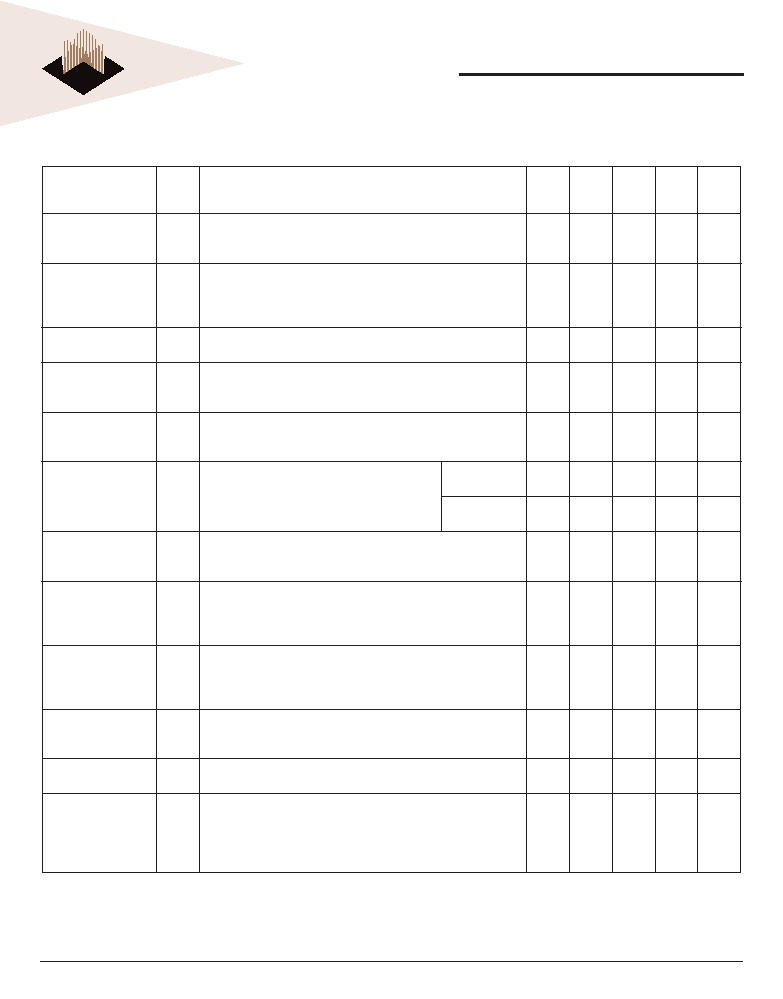
DDR2 IDD SPECIFICATIONS AND CONDITIONS
DDR2 SDRAM components only
Parameter
Active
Rank
State
Condition
806
665
553
403
Units
Operating one device
bank active-precharge
current;
IDD0
tCK = tCK (IDD), tRC = tRC (IDD), tRAS = tRAS MIN (IDD); CKE is HIGH, S# is
HIGH between valid commands; Address bus inputs are SWITCHING;
Data bus inputs are SWITCHING.
TBD
720
640
mA
Operating one device
bank active-read-
precharge current;
IDD1
IOUT = 0mA; BL = 4, CL = CL(IDD), AL = 0; tCK = tCK (IDD), tRC = tRC
(IDD), tRAS = tRAS MIN (IDD), tRCD = tRCD (IDD); CKE is HIGH, S# is HIGH
between valid commands; Address bus inputs are SWITCHING; Data
pattern is same as IDD4W.
TBD
840
760
720
mA
Precharge power-down
current;
IDD2P
All device banks idle; tCK = tCK (IDD); CKE is LOW; Other control and
address bus inputs are STABLE; Data bus inputs are FLOATING.
TBD
40
mA
Precharge quiet
standby current;
IDD2Q
All device banks idle; tCK = tCK (IDD); CKE is HIGH, S# is HIGH; Other
control and address bus inputs are STABLE; Data bus inputs are
FLOATING.
TBD
400
320
280
mA
Precharge standby
current;
IDD2N
All device banks idle; tCK = tCK (IDD); CKE is HIGH, S# is HIGH; Other
control and address bus inputs are SWITCHING; Data bus inputs are
SWITCHING.
TBD
440
360
320
mA
Active power-down
current;
IDD3P
All device banks open; tCK = tCK (IDD); CKE is LOW;
Other control and address bus inputs are STABLE;
Data bus inputs are FLOATING.
Fast PDN Exit
MR[12] = 0
TBD
280
240
200
mA
Slow PDN Exit
MR[12] = 1
TBD
80
mA
Active standby current;
IDD3N
All device banks open; tCK = tCK(IDD), tRAS = tRAS MAX (IDD), tRP = tRP(IDD);
CKE is HIGH, S# is HIGH between valid commands; Other control and
address bus inputs are SWITCHING; Data bus inputs are SWITCHING.
TBD
520
440
360
mA
Operating burst write
current;
IDD4W
All device banks open, Continuous burst writes; BL = 4, CL = CL (IDD),
AL = 0; tCK = tCK (IDD), tRAS = tRAS MAX (IDD), tRP = tRP (IDD); CKE is
HIGH, S# is HIGH between valid commands; Address bus inputs are
SWITCHING; Data bus inputs are SWITCHING.
TBD
1,240
1,040
880
mA
Operating burst read
current;
IDD4R
All device banks open, Continuous burst reads, IOUT = 0mA; BL = 4, CL
= CL (IDD), AL = 0; tCK = tCK (IDD), tRAS = tRAS MAX (IDD), tRP = tRP (IDD);
CKE is HIGH, S# is HIGH between valid commands; Address bus inputs
are SWITCHING; Data bus inputs are SWITCHING.
TBD
1,400
1,160
920
mA
Burst refresh current;
IDD5
tCK = tCK (IDD); Refresh command at every tRFC (IDD) interval; CKE is
HIGH, S# is HIGH between valid commands; Other control and address
bus inputs are SWITCHING; Data bus inputs are SWITCHING.
TBD
1,680
1,600
1, 520
mA
Self refresh current;
IDD6
CK and CK# at 0V; CKE ≤ 0.2V; Other control and address bus inputs
are FLOATING; Data bus inputs are FLOATING.
TBD
40
mA
Operating device bank
interleave read current;
IDD7
All device banks interleaving reads, IOUT= 0mA; BL = 4, CL = CL (IDD),
AL = tRCD (IDD)-1 x tCK (IDD); tCK = tCK (IDD), tRC = tRC(IDD), tRRD = tRRD(IDD),
tRCD = tRCD(IDD); CKE is HIGH, S# is HIGH between valid commands;
Address bus inputs are STABLE during DESELECTs; Data bus inputs
are SWITCHING; See IDD7 Conditions for detail.
TBD
2,240
2,080
1,840
mA
Note:
IDD specication is based on
MICRON components. Other DRAM manufactures specication may be different.
相關(guān)PDF資料 |
PDF描述 |
|---|---|
| W7NCF512H10CS7JM1G | FLASH 3.3V PROM MODULE, XMA50 |
| W7NCF512H10CSA3CM1G | FLASH 3.3V PROM MODULE, XMA50 |
| W7NCF512H10CSA9DM1G | FLASH 3.3V PROM MODULE, XMA50 |
| W7NCF512H10IS9DM1G | FLASH 3.3V PROM MODULE, XMA50 |
| W7NCF512H10ISA2HM1G | FLASH 3.3V PROM MODULE, XMA50 |
相關(guān)代理商/技術(shù)參數(shù) |
參數(shù)描述 |
|---|---|
| W3HG64M72EER403AD7XG | 制造商:WEDC 制造商全稱:White Electronic Designs Corporation 功能描述:512MB - 64Mx72 DDR2 SDRAM REGISTERED, w/PLL, VLP Mini-DIMM |
| W3HG64M72EER534AD7XG | 制造商:WEDC 制造商全稱:White Electronic Designs Corporation 功能描述:512MB - 64Mx72 DDR2 SDRAM REGISTERED, w/PLL, VLP Mini-DIMM |
| W3HG64M72EER665AD7XG | 制造商:WEDC 制造商全稱:White Electronic Designs Corporation 功能描述:512MB - 64Mx72 DDR2 SDRAM REGISTERED, w/PLL, VLP Mini-DIMM |
| W3HG64M72EER806AD7XG | 制造商:WEDC 制造商全稱:White Electronic Designs Corporation 功能描述:512MB - 64Mx72 DDR2 SDRAM REGISTERED, w/PLL, VLP Mini-DIMM |
| W3HG64M72EER-AD7 | 制造商:WEDC 制造商全稱:White Electronic Designs Corporation 功能描述:512MB - 64Mx72 DDR2 SDRAM REGISTERED, w/PLL, VLP Mini-DIMM |
發(fā)布緊急采購(gòu),3分鐘左右您將得到回復(fù)。