- 您現(xiàn)在的位置:買賣IC網(wǎng) > PDF目錄379478 > UCC2941-ADJ (Electronic Theatre Controls, Inc.) 1V Synchronous Boost Converter PDF資料下載
參數(shù)資料
| 型號(hào): | UCC2941-ADJ |
| 廠商: | Electronic Theatre Controls, Inc. |
| 英文描述: | 1V Synchronous Boost Converter |
| 中文描述: | 1V的同步升壓轉(zhuǎn)換器 |
| 文件頁(yè)數(shù): | 1/8頁(yè) |
| 文件大小: | 143K |
| 代理商: | UCC2941-ADJ |
UCC19411/2/3
UCC29411/2/3
UCC39411/2/3
PRELIMINARY
DESCRIPTION
The UCC39411 family of
converters is optimized to operate from a single or dual alkaline cell, and
steps up to a 3.3V, 5V, or adjustable output at 200mW. The UCC39411
family also provides an auxiliary 7V output, primarily for the gate drive
supply, which can be used for applications requiring an auxiliary output,
such as 5V, by linear regulating. The primary output will start up under full
load at input voltages typically as low as 0.8V with a guaranteed max of
1V, and will operate down to 0.5V once the converter is operating,
maximizing battery utilization.
low input voltage, single inductor boost
The
applications such as pagers and cell phones that require high efficiency
over a wide operating range of several milli-watts to a couple of hundred
milli-watts. High efficiency at low output current is achieved by optimizing
switching and conduction losses with a low total quiescent current (50
μ
A).
At higher output current the 0.5
switch, and 1.2
synchronous rectifier
along with continuous mode conduction provide high power efficiency. The
wide input voltage range of the UCC39411 family can accommodate other
power sources such as NiCd and NimH.
UCC39411
family
is
designed
to
accommodate
demanding
The 39411 family also provides shutdown control. Packages available are
the 8 pin SOIC (D), 8 pin DIP (N or J), and 8 pin TSSOP (PW) to optimize
board space.
Low Power Synchronous Boost Converter
FEATURES
1V Input Voltage Operation Start-up
Guaranteed under FULL Load on
Main Output, and Operation Down to
0.5V
200mW Output Power at Battery
Voltages as low as 0.8V
Secondary 7V Supply from a Single
Inductor
Output Fully Disconnected in
Shutdown
Adaptive Current Mode Control for
Optimum Efficiency
High Efficiency over Wide Operating
Range
6
μ
A Shutdown Supply Current
Output Reset Function with
Programmable Reset Period
SLUS245A - MARCH 1999
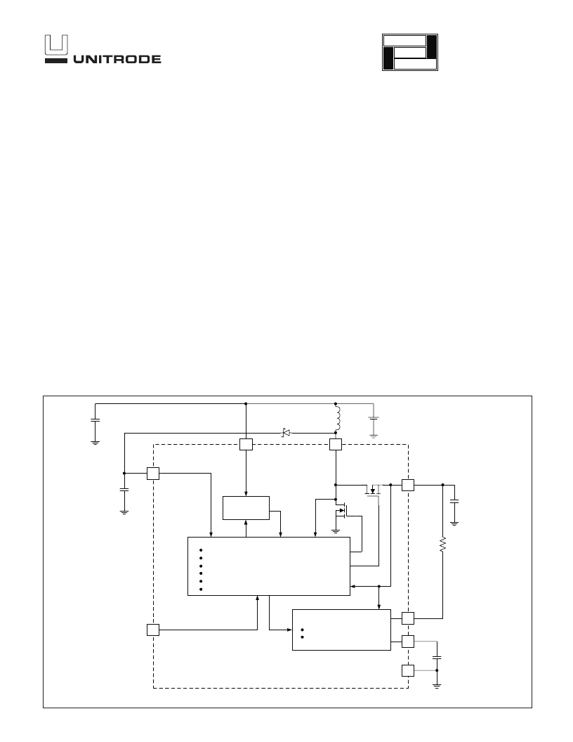
1
4
7
6
VOUT
GND
3.3V 200mW
5
C
T
R
RES
3
100
μ
F
RESET CONTROL CIRCUIT
GLITCH SUPRESSION
PROGRAMMABLE TIMING
MODULATOR CONTROL CIRCUIT
SYNCHRONOUS RECTIFICATION CIRCUITRY
ANTI-CROSS CONDUCTION
START-UP
MULTIPLEXING LOGIC
MAX INPUT POWER CONTROL
ADAPTIVE CURRENT CONTROL
START-UP
CIRCUITRY
1.2
CT
RESB
2
SD/FB
100
μ
F
VIN
SW
8
VGD
0.5
100
μ
F
1V TO 3.5V
22
μ
H
+
SIMPIFIED BLOCK DIAGRAM AND APPLICATION CIRCUIT (UCC39412)
UDG-98067
Note: Pinout shown is for the TSSOP Package. Consult Package Descriptions for DIP and SOIC configurations.
application
INFO
available
相關(guān)PDF資料 |
PDF描述 |
|---|---|
| UCC1946 | R8C Series, 20 Group, WDTO 48P6Q-A |
| UCC1972 | R8C Series, 20 Group, WDTO 48P6Q-A |
| UCC1973 | R8C Series, 20 Group, WDTO 48P6Q-A |
| UCC2752 | TOOLS,KITS,ELECTRONIC,NETWORK KIT, 22 PCS,COMPUTER ACCESSORIES,NETWORK MAINTENANCE KIT ,SPC TECHNOLOGY RoHS Compliant: NA |
| UCC28089DRB | PRIMARY-SIDE PUSH-PULL OSCILLATOR WITH DEAD-TIME CONTROL |
相關(guān)代理商/技術(shù)參數(shù) |
參數(shù)描述 |
|---|---|
| UCC2941D-3 | 制造商:Rochester Electronics LLC 功能描述:- Bulk |
| UCC2941ND-3 WAF | 制造商:Texas Instruments 功能描述: |
| UCC2941ND-5 WAF | 制造商:Texas Instruments 功能描述: |
| UCC2941ND-ADJ WAF | 制造商:Texas Instruments 功能描述: |
| UCC29421N | 功能描述:DC/DC 開(kāi)關(guān)控制器 High Freq Multimode Sync Controller RoHS:否 制造商:Texas Instruments 輸入電壓:6 V to 100 V 開(kāi)關(guān)頻率: 輸出電壓:1.215 V to 80 V 輸出電流:3.5 A 輸出端數(shù)量:1 最大工作溫度:+ 125 C 安裝風(fēng)格: 封裝 / 箱體:CPAK |
發(fā)布緊急采購(gòu),3分鐘左右您將得到回復(fù)。