- 您現(xiàn)在的位置:買賣IC網(wǎng) > PDF目錄379478 > UCC28089DRB (Texas Instruments, Inc.) PRIMARY-SIDE PUSH-PULL OSCILLATOR WITH DEAD-TIME CONTROL PDF資料下載
參數(shù)資料
| 型號: | UCC28089DRB |
| 廠商: | Texas Instruments, Inc. |
| 英文描述: | PRIMARY-SIDE PUSH-PULL OSCILLATOR WITH DEAD-TIME CONTROL |
| 中文描述: | 一次側(cè)推拉振蕩器死區(qū)時間控制 |
| 文件頁數(shù): | 6/19頁 |
| 文件大小: | 336K |
| 代理商: | UCC28089DRB |
SLUS623 SEPTEMBER 2004
6
www.ti.com
APPLICATION INFORMATION
UCC28089 is an alternating dual-driver output oscillator with over-current and under-voltage fault protection.
This feature set is ideal as a start-up controller for isolated power systems where the majority of control functions
are performed on the secondary side. This device is especially useful for dc link for topologies such as the
cascaded buck converter [1], ac link inverter topologies [2], and inexpensive modified square wave inverters.
The UCC28089 has a brief 5 to 7 cycle leading-edge modulated soft-start cycle so that it will not interfere with
secondary-side controlled soft start. Both systems with off-line self bias and auxiliary bias supplies are more
fault tolerant with the UCC28089 because it consistently responds to a fault with a delay of at least 56 oscillator
cycles before retry.
Detailed Functional Description
VDD:
Power input connection for this device. Although quiescent VDD current is very low, total supply current
is higher, depending on OUTA and OUTB current and the programmed oscillator frequency. During fault
response, the current drops to a lower level because the oscillator is disabled.
In order to avoid noise problems, position a 1-
μ
F ceramic bypass capacitor, connected from VDD to GND, as
close to the chip as possible. The ceramic bypass capacitor is in addition to any energy storage capacitance
that would be used to hold up the VDD voltage during start-up transients.
GND:
Ground pin. Analog signals reference this pin and output drivers return current through this pin. For best
results, use this pin as a local ground point in a star ground configuration.
OUTA and OUTB:
Output drivers capable of sinking 1 A and sourcing 0.5 A. The output pulse alternates
between OUTA and OUTB. In addition, a T latch forces the output pulses to alternate in order to reduce flux build
up in a transformer during low duty ratio operation. Each output is capable of driving the gate of a power
MOSFET.
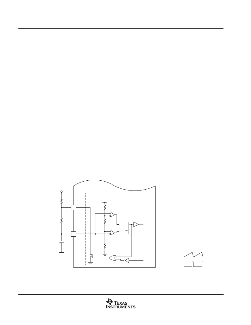
CT and DIS:
Oscillator timing capacitor pin and timing capacitor discharge pin. The UCC28089 oscillator tracks
VDD and GND internally in order to minimize oscillator frequency changes due to variations in the voltage of
VDD. Figure 1 shows the oscillator block diagram.
2
DIS
3
CT
RA
RB
CT
VDD
OSCILLATOR
D
Q
R
VROK
CK
VDD
15.7Rx
2.90Rx
Rx
UCC28089
VDD/19.6
VDD/5
V(CT)
CK
Figure 1. Block Diagram for Oscillator
相關(guān)PDF資料 |
PDF描述 |
|---|---|
| UCC2813-0QDRQ1 | LOW-POWER BICMOS CURRENT-MODE PWM |
| UCC2813PWTR-2 | Low Power Economy BiCMOS Current Mode PWM |
| UCC2813NTR-0 | Low Power Economy BiCMOS Current Mode PWM |
| UCC2813NTR-1 | Low Power Economy BiCMOS Current Mode PWM |
| UCC2813-2QDRQ1 | LOW-POWER BICMOS CURRENT-MODE PWM |
相關(guān)代理商/技術(shù)參數(shù) |
參數(shù)描述 |
|---|---|
| UCC28089DRBR | 制造商:Texas Instruments 功能描述:PRIMARY SIDE PUSH-PULL DRIVER WITH DEAD-TIME CONTROL - Tape and Reel |
| UCC28089DRBT | 制造商:Rochester Electronics LLC 功能描述:- Bulk |
| UCC28089DRG4 | 功能描述:功率驅(qū)動器IC Primary Side P-P Driver RoHS:否 制造商:Micrel 產(chǎn)品:MOSFET Gate Drivers 類型:Low Cost High or Low Side MOSFET Driver 上升時間: 下降時間: 電源電壓-最大:30 V 電源電壓-最小:2.75 V 電源電流: 最大功率耗散: 最大工作溫度:+ 85 C 安裝風(fēng)格:SMD/SMT 封裝 / 箱體:SOIC-8 封裝:Tube |
| UCC2808A-1 | 制造商:TI 制造商全稱:Texas Instruments 功能描述:LOW POWER CURRENT MODE PUSH-PULL PWM |
| UCC2808A-1EP | 制造商:TI 制造商全稱:Texas Instruments 功能描述:LOW POWER CURRENT MODE PUSH-PULL PWM |
發(fā)布緊急采購,3分鐘左右您將得到回復(fù)。