- 您現(xiàn)在的位置:買賣IC網(wǎng) > PDF目錄385952 > TWL1110TQFP (Texas Instruments, Inc.) VOICE-BAND AUDIO PROCESSOR VBAPE PDF資料下載
參數(shù)資料
| 型號: | TWL1110TQFP |
| 廠商: | Texas Instruments, Inc. |
| 英文描述: | VOICE-BAND AUDIO PROCESSOR VBAPE |
| 中文描述: | 語音頻帶音頻處理器VBAPE |
| 文件頁數(shù): | 10/37頁 |
| 文件大小: | 496K |
| 代理商: | TWL1110TQFP |
第1頁第2頁第3頁第4頁第5頁第6頁第7頁第8頁第9頁當(dāng)前第10頁第11頁第12頁第13頁第14頁第15頁第16頁第17頁第18頁第19頁第20頁第21頁第22頁第23頁第24頁第25頁第26頁第27頁第28頁第29頁第30頁第31頁第32頁第33頁第34頁第35頁第36頁第37頁
TWL1110
VOICE-BAND AUDIO PROCESSOR (VBAP
)
SLWS103 – NOVEMBER 2000
10
POST OFFICE BOX 655303
DALLAS, TEXAS 75265
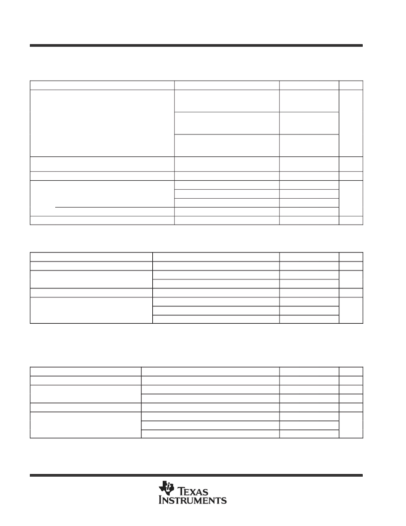
electrical characteristics over recommended ranges of supply voltage and free-air temperature (unless
otherwise noted) (continued)
speaker interface
PARAMETER
TEST CONDITIONS
MIN
TYP
MAX
UNIT
VDD = 2.7 V, fully differential, 8-
load,
3-dBm0 output, volume control = –3 dB,
RXPGA = –4 dB level
VDD = 2.7 V, fully differential, 16-
load,
3-dBm0 output, volume control = –3 dB,
RXPGA = –2 dB level
VDD = 2.7 V, fully differential, 32-
load,
3-dBm0 output, volume control = –3 dB,
RXPGA = –1 dB level
VDD = 2.7 V, single-ended, 32-
load,
3-dBm0 output
161
200
Earphone AMP1 output power (see Note 6)
128
160
mW
81
100
Earphone AMP2 output power (see Note 6)
10
12.5
mW
VOO
Output offset voltage at EAR1
Fully differential
3-dBm0 input, 8-
load
3-dBm0 input, 16-
load
3-dBm0 input, 32-
load
3-dBm0 input
±
5
141
±
30
178
mV
I max
IOmax
Maximum output current for EAR1 (rms)
Maximum out ut current for EAR1 (rms)
90
112
mA
50
63
Maximum output current for EAR2 (rms)
17.7
22.1
EARMUTE
–80
dB
NOTE 6: Maximum power is with a load impedance of –25%.
transmit gain and dynamic range, companded mode (
μ
-law or A-law) or linear mode selected, transmit slope
filter bypassed (see Notes 7 and 8)
PARAMETER
TEST CONDITIONS
MIN
TYP
MAX
UNIT
Transmit reference-signal level (0 dB)
Differential
87.5
mVpp
Overload signal level (3 dBm0)
Overload-signal level (3 dBm0)
Differential, normal mode
124
mVpp
Differential, extended mode
0 dBm0 input signal, VDD
±
10%
MIC1N, MIC1P to PCMO at 3 dBm0 to –30 dBm0
31.5
Absolute gain error
–1
1
dB
G i
–10 dBm0 MIC1N MIC1P to PCMO
–10 dBm0 MIC1N, MIC1P to PCMO
ith i
t l
l
l ti
t
i
t
–0.5
0.5
MIC1N, MIC1P to PCMO at –31 dBm0 to –45 dBm0
MIC1N, MIC1P to PCMO at –46 dBm0 to –55 dBm0
–1
1
dB
–1.2
1.2
NOTES:
7. Unless otherwise noted, the analog input is 0 dB, 1020-Hz sine wave, where 0 dB is defined as the zero-reference point of the channel
under test.
8. The reference signal level, which is input to the transmit channel, is defined as a value 3 dB below the full-scale value of 88-mVrms.
transmit gain and dynamic range, companded mode (
μ
-law or A-law) or linear mode selected, transmit slope
filter enabled (see Notes 7 and 8)
PARAMETER
TEST CONDITIONS
MIN
TYP
MAX
UNIT
Transmit reference-signal level (0 dB)
Differential
87.5
mVpp
mVpp
mVpp
dB
Overload signal level (3 dBm0)
Overload-signal level (3 dBm0)
Differential, normal mode
124
Differential, extended mode
0 dBm0 input signal, VDD
±
10%
MIC1N, MIC1P to PCMO at 3 dBm0 to –30 dBm0
31.5
Absolute gain error
–1
1
G i
Gain error with input level relative to gain at
–10 dBm0 MIC1N MIC1P to PCMO
–10 dBm0 MIC1N, MIC1P to PCMO
l ti
–0.5
0.5
MIC1N, MIC1P to PCMO at –31 dBm0 to –45 dBm0
–1
1
dB
MIC1N, MIC1P to PCMO at –46 dBm0 to –55 dBm0
–1.2
1.2
NOTES:
7. Unless otherwise noted, the analog input is 0 dB, 1020-Hz sine wave, where 0 dB is defined as the zero-reference point of the
channel under test.
8 The reference signal level, which is input to the transmit channel, is defined as a value 3 dB below the full-scale value of 88-mVrms.
相關(guān)PDF資料 |
PDF描述 |
|---|---|
| TX45 | HIGH-ENERGY TRIGGERED SPARK GAPS |
| XA1000 | DC-18.0 GHz GaAs MMIC 5-Bit Digital Attenuator |
| XAUR13C | 12.7mm (0.5 inch) 16 SEGMENT SINGLE DIGIT ALPHANUMERIC DISPLAY |
| XB1002 | 36.0-43.0 GHz GaAs MMIC Buffer Amplifier |
| XB1004 | 16.0-30.0 GHz GaAs MMIC Buffer Amplifier |
相關(guān)代理商/技術(shù)參數(shù) |
參數(shù)描述 |
|---|---|
| TWL1200 | 制造商:TI 制造商全稱:Texas Instruments 功能描述:SDIO, UART, AND AUDIO VOLTAGE-TRANSLATION TRANSCEIVER |
| TWL1200IPFBRQ1 | 功能描述:轉(zhuǎn)換 - 電壓電平 SDIO,UART,and Audio Vltg-Level Xcvr RoHS:否 制造商:Micrel 類型:CML/LVDS/LVPECL to LVCMOS/LVTTL 傳播延遲時間:1.9 ns 電源電流:14 mA 電源電壓-最大:3.6 V 電源電壓-最小:3 V 最大工作溫度:+ 85 C 安裝風(fēng)格:SMD/SMT 封裝 / 箱體:MLF-8 |
| TWL1200-Q1 | 制造商:TI 制造商全稱:Texas Instruments 功能描述:SDIO, UART, AND AUDIO VOLTAGE-TRANSLATION TRANSCEIVER |
| TWL1200YFFR | 功能描述:轉(zhuǎn)換 - 電壓電平 SDIO UART & Aud Vltg Level Transceiver RoHS:否 制造商:Micrel 類型:CML/LVDS/LVPECL to LVCMOS/LVTTL 傳播延遲時間:1.9 ns 電源電流:14 mA 電源電壓-最大:3.6 V 電源電壓-最小:3 V 最大工作溫度:+ 85 C 安裝風(fēng)格:SMD/SMT 封裝 / 箱體:MLF-8 |
| TWL1200ZQCR | 功能描述:轉(zhuǎn)換 - 電壓電平 SDIO UART & Audio Vltg-Level Xcvr RoHS:否 制造商:Micrel 類型:CML/LVDS/LVPECL to LVCMOS/LVTTL 傳播延遲時間:1.9 ns 電源電流:14 mA 電源電壓-最大:3.6 V 電源電壓-最小:3 V 最大工作溫度:+ 85 C 安裝風(fēng)格:SMD/SMT 封裝 / 箱體:MLF-8 |
發(fā)布緊急采購,3分鐘左右您將得到回復(fù)。