- 您現(xiàn)在的位置:買賣IC網(wǎng) > PDF目錄368672 > TMS320F240PQS 16-Bit Microcontroller PDF資料下載
參數(shù)資料
| 型號: | TMS320F240PQS |
| 英文描述: | 16-Bit Microcontroller |
| 中文描述: | 16位微控制器 |
| 文件頁數(shù): | 94/105頁 |
| 文件大小: | 1481K |
| 代理商: | TMS320F240PQS |
第1頁第2頁第3頁第4頁第5頁第6頁第7頁第8頁第9頁第10頁第11頁第12頁第13頁第14頁第15頁第16頁第17頁第18頁第19頁第20頁第21頁第22頁第23頁第24頁第25頁第26頁第27頁第28頁第29頁第30頁第31頁第32頁第33頁第34頁第35頁第36頁第37頁第38頁第39頁第40頁第41頁第42頁第43頁第44頁第45頁第46頁第47頁第48頁第49頁第50頁第51頁第52頁第53頁第54頁第55頁第56頁第57頁第58頁第59頁第60頁第61頁第62頁第63頁第64頁第65頁第66頁第67頁第68頁第69頁第70頁第71頁第72頁第73頁第74頁第75頁第76頁第77頁第78頁第79頁第80頁第81頁第82頁第83頁第84頁第85頁第86頁第87頁第88頁第89頁第90頁第91頁第92頁第93頁當(dāng)前第94頁第95頁第96頁第97頁第98頁第99頁第100頁第101頁第102頁第103頁第104頁第105頁
TMS320C240, TMS320F240
DSP CONTROLLERS
SPRS042D – OCTOBER 1996 – REVISED NOVEMBER 1998
94
POST OFFICE BOX 1443
HOUSTON, TEXAS 77251–1443
operating characteristics over recommended operating condition ranges
PARAMETER
DESCRIPTION
MIN
MAX
UNIT
VCCA= 5 5 V
VCCA = 5.5 V
converting
5
ICCA
Analog supply current
non-converting
2
mA
VCCA = VREFHI = 5.5 V
PLL or OSC power
down
1
Iref
Input charge current, VREFHI or VREFLO
VCCA = VCCD = VREFHI = 5.5 V, VREFLO = 0 V
Typical capacitive load on
analog input pin
5
mA
Ci
Cai
Analog input capacitance
non-sampling
6
pF
sampling
8
ZAI
Analog input source impedance
Analog input source impedance for conversions to
remain within specifications.
9
k
EDNL
Differential nonlinearity error
Difference between the actual step width and the ideal
value
– 1
1.5
LSB
EINL
Integral nonlinearity error
Maximum deviation from the best straight line through
the ADC transfer characteristics, excluding the
quantization error
1.5
LSB
td(PU)
Absolute resolution = 4.89 mV. At VREFHI = 5 V and VREFLO = 0 V, this s one LSB. As VREFHI decreases, VREFLO ncreases, or both, he LSB sizes
decrease. Therefore, the absolute accuracy and differential/integral linearity errors in terms of LSBs increase.
Delay time, power-up to ADC valid
Time to stabilize analog stage after power-up
10
s
The ADC module allows complete freedom in the design of the sources for the analog inputs. The period of the
sample time is independent of the source impedance. The sample-and-hold period occurs in the first half-period
of the ADC clock after the ADCIMSTART bit or the ADCSOC bit of the ADC control register 1 (ADCTRL1, bits 13
and 0, respectively) is set to 1. The conversion then occurs during the next six ADC clock cycles. The digital
result registers are updated on the next ADC clock cycle once the conversion is completed.
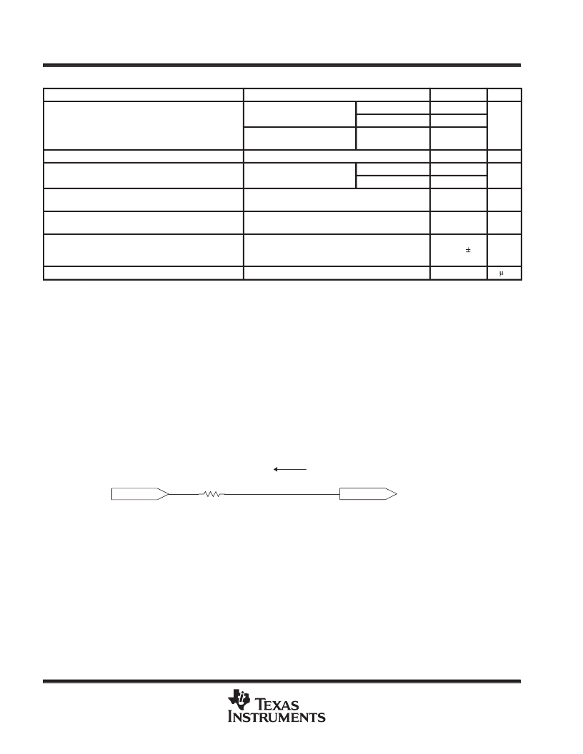
ADC input pin circuit
One of the most common A/D application errors is inappropriate source impedance. In practice, minimum
source impedance should be used to limit the error as well as minimize the required sampling time; however,
the source impedance must be smaller than Z
AI
. A typical ADC input pin circuit is shown in Figure 47.
VIN
R1
Requiv
VAI
(to ADCINx input)
R1 = 9 k
typical
Figure 47. Typical ADC Input Pin Circuit
相關(guān)PDF資料 |
PDF描述 |
|---|---|
| TMS320LC31-40 | Digital Signal Processor |
| TMS320LC53PQ | 16-Bit Digital Signal Processor |
| TMP320C51HQ | Transient Voltage Suppressor Diodes |
| TMS320C50PQA40 | 16-Bit Digital Signal Processor |
| TMS320C51PQA40 | 16-Bit Digital Signal Processor |
相關(guān)代理商/技術(shù)參數(shù) |
參數(shù)描述 |
|---|---|
| TMS320F241FN | 功能描述:數(shù)字信號處理器和控制器 - DSP, DSC 16B 5V fixed point DSP w/ Flash RoHS:否 制造商:Microchip Technology 核心:dsPIC 數(shù)據(jù)總線寬度:16 bit 程序存儲器大小:16 KB 數(shù)據(jù) RAM 大小:2 KB 最大時鐘頻率:40 MHz 可編程輸入/輸出端數(shù)量:35 定時器數(shù)量:3 設(shè)備每秒兆指令數(shù):50 MIPs 工作電源電壓:3.3 V 最大工作溫度:+ 85 C 封裝 / 箱體:TQFP-44 安裝風(fēng)格:SMD/SMT |
| TMS320F241FN | 制造商:Texas Instruments 功能描述:IC C2000 DSP SMD 320F241 PLCC68 |
| TMS320F241FNA | 功能描述:數(shù)字信號處理器和控制器 - DSP, DSC 16B 5V fixed point DSP w/ Flash RoHS:否 制造商:Microchip Technology 核心:dsPIC 數(shù)據(jù)總線寬度:16 bit 程序存儲器大小:16 KB 數(shù)據(jù) RAM 大小:2 KB 最大時鐘頻率:40 MHz 可編程輸入/輸出端數(shù)量:35 定時器數(shù)量:3 設(shè)備每秒兆指令數(shù):50 MIPs 工作電源電壓:3.3 V 最大工作溫度:+ 85 C 封裝 / 箱體:TQFP-44 安裝風(fēng)格:SMD/SMT |
| TMS320F241FNS | 功能描述:數(shù)字信號處理器和控制器 - DSP, DSC 16B 5V fixed point DSP w/ Flash RoHS:否 制造商:Microchip Technology 核心:dsPIC 數(shù)據(jù)總線寬度:16 bit 程序存儲器大小:16 KB 數(shù)據(jù) RAM 大小:2 KB 最大時鐘頻率:40 MHz 可編程輸入/輸出端數(shù)量:35 定時器數(shù)量:3 設(shè)備每秒兆指令數(shù):50 MIPs 工作電源電壓:3.3 V 最大工作溫度:+ 85 C 封裝 / 箱體:TQFP-44 安裝風(fēng)格:SMD/SMT |
| TMS320F241PG | 功能描述:數(shù)字信號處理器和控制器 - DSP, DSC 16B 5V fixed point DSP w/ Flash RoHS:否 制造商:Microchip Technology 核心:dsPIC 數(shù)據(jù)總線寬度:16 bit 程序存儲器大小:16 KB 數(shù)據(jù) RAM 大小:2 KB 最大時鐘頻率:40 MHz 可編程輸入/輸出端數(shù)量:35 定時器數(shù)量:3 設(shè)備每秒兆指令數(shù):50 MIPs 工作電源電壓:3.3 V 最大工作溫度:+ 85 C 封裝 / 箱體:TQFP-44 安裝風(fēng)格:SMD/SMT |
發(fā)布緊急采購,3分鐘左右您將得到回復(fù)。