- 您現(xiàn)在的位置:買賣IC網(wǎng) > PDF目錄98258 > TLV5614IYZR (TEXAS INSTRUMENTS INC) SERIAL INPUT LOADING, 9 us SETTLING TIME, 12-BIT DAC, UUC16 PDF資料下載
參數(shù)資料
| 型號: | TLV5614IYZR |
| 廠商: | TEXAS INSTRUMENTS INC |
| 元件分類: | DAC |
| 英文描述: | SERIAL INPUT LOADING, 9 us SETTLING TIME, 12-BIT DAC, UUC16 |
| 封裝: | GREEN, DIE-16 |
| 文件頁數(shù): | 20/25頁 |
| 文件大小: | 500K |
| 代理商: | TLV5614IYZR |
www.ti.com
h(D)
1
2
3
4
5
15
16
D15
D14
D13
D12
D1
D0
t
su(FS-CK)
t
su(CS-FS)
t
wH(FS)
t
su(D)
t
wH
t
wL
t
su(C16-FS)
SCLK
DIN
CS
FS
t
su(C16-CS)
SBAS401 – DECEMBER 2006
ELECTRICAL CHARACTERISTICS (continued)
Over operating free-air temperature range, supply voltages, and reference voltages (unless otherwise noted).
PARAMETER
TEST CONDITIONS
MIN
TYP
MAX
UNIT
ANALOG OUTPUT DYNAMIC PERFORMANCE
Fast
5
V/
s
CL = 100pF, RL = 10k, VO = 10% to 90%,
SR
Output slew rate
VREF = 2.048V, 1024V
Slow
1
V/
s
Fast
3
5.5
To
± 0.5 LSB, C
L = 100pF, RL = 10k, see
ts
Output settling time
s
(11) (12)
Slow
9
20
Fast
1
To
± 0.5 LSB, C
L = 100pF, RL = 10k, see
ts(c)
Output settling time, code to code
s
(13)
Slow
2
Glitch energy
Code transition from 7FF to 800
10
nV–s
SNR
Signal-to-noise ratio
74
Sinewave generated by DAC, Reference voltage =
SINAD
Signal to noise + distortion
66
1.024 at 3V and 2.048 at 5V, fS = 400KSPS, fOUT =
dB
1.1kHz sinewave, CL = 100pF, RL = 10k, BW =
THD
Total harmonic distortion
–68
20kHz
SFDR
Spurious-free dynamic range
70
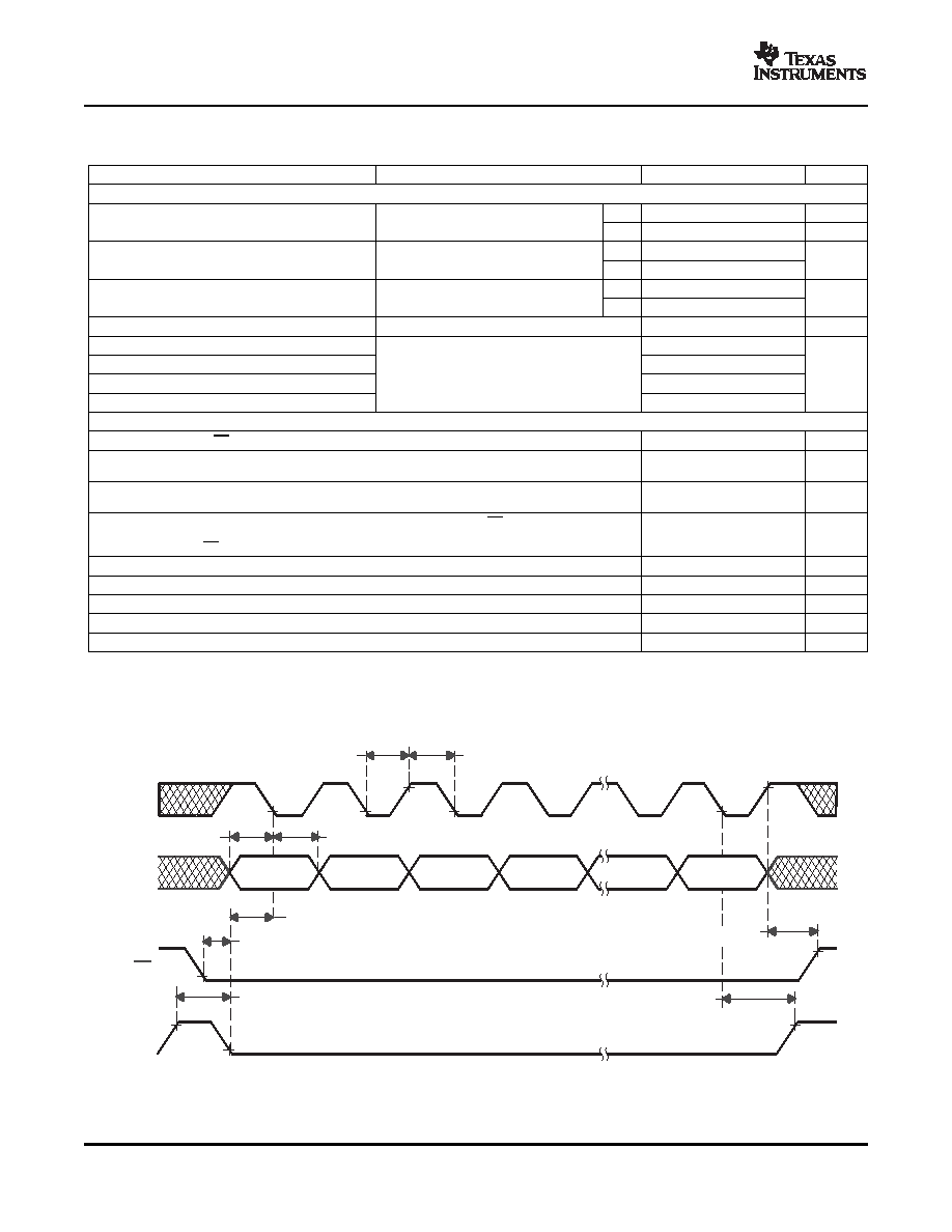
DIGITAL INPUT TIMING REQUIREMENTS
tsu(CS–FS)
Setup time, CS low before FS
↓
10
ns
Setup time, FS low before first negative
tsu(FS–CK)
SCLK edge
8
ns
Setup time. 16th negative SCLK edge after FS low on which bit D0 is sampled before rising edge
tsu(C16–FS)
of FS
10
ns
Setup time. The first positive SCLK edge after D0 is sampled before CS rising edge. If FS is used
instead of the SCLK positive edge to update the DAC, then the setup time is between the FS rising
tsu(C16–CS)
edge and CS rising edge.
10
ns
twH
Pulse duration, SCLK high
25
ns
twL
Pulse duration, SCLK low
25
ns
tsu(D)
Setup time, data ready before SCLK falling edge
8
ns
th(D)
Hold time, data held valid after SCLK falling edge
5
ns
twH(FS)
Pulse duration, FS high
20
ns
(11) Settling time is the time for the output signal to remain within
±0.5 LSB of the final measured value for a digital input code change of
FFFhex to 080hex for 080hex to FFFhex.
(12) Limits are ensured by design and characterization, but are not production tested.
(13) Settling time is the time for the output signal to remain within
±0.5 LSB of the final measured value for a digital input code change of one
count.
Figure 1. Timing Diagram
4
相關(guān)PDF資料 |
PDF描述 |
|---|---|
| TLV5614IYZT | SERIAL INPUT LOADING, 9 us SETTLING TIME, 12-BIT DAC, UUC16 |
| TLV5614MPWREP | SERIAL INPUT LOADING, 9 us SETTLING TIME, 12-BIT DAC, PDSO16 |
| TLV5616CDGKRG4 | SERIAL INPUT LOADING, 9 us SETTLING TIME, 12-BIT DAC, PDSO8 |
| TLV5616CDR | SERIAL INPUT LOADING, 9 us SETTLING TIME, 12-BIT DAC, PDSO8 |
| TLV5616CD | SERIAL INPUT LOADING, 9 us SETTLING TIME, 12-BIT DAC, PDSO8 |
相關(guān)代理商/技術(shù)參數(shù) |
參數(shù)描述 |
|---|---|
| TLV5614IYZT | 功能描述:數(shù)模轉(zhuǎn)換器- DAC 2.7V-5.5V 12B lead free/green DAC RoHS:否 制造商:Texas Instruments 轉(zhuǎn)換器數(shù)量:1 DAC 輸出端數(shù)量:1 轉(zhuǎn)換速率:2 MSPs 分辨率:16 bit 接口類型:QSPI, SPI, Serial (3-Wire, Microwire) 穩(wěn)定時(shí)間:1 us 最大工作溫度:+ 85 C 安裝風(fēng)格:SMD/SMT 封裝 / 箱體:SOIC-14 封裝:Tube |
| TLV5614MPWREP | 功能描述:數(shù)模轉(zhuǎn)換器- DAC Mil Enhance Quad DAC Ser In Lo-pwr RoHS:否 制造商:Texas Instruments 轉(zhuǎn)換器數(shù)量:1 DAC 輸出端數(shù)量:1 轉(zhuǎn)換速率:2 MSPs 分辨率:16 bit 接口類型:QSPI, SPI, Serial (3-Wire, Microwire) 穩(wěn)定時(shí)間:1 us 最大工作溫度:+ 85 C 安裝風(fēng)格:SMD/SMT 封裝 / 箱體:SOIC-14 封裝:Tube |
| TLV5614PW | 制造商:TI 制造商全稱:Texas Instruments 功能描述:2.7-V TO 5.5-V 12-BIT 3-mS QUADRUPLE DIGITAL-TO-ANALOG CONVERTERS WITH POWER DOWN |
| TLV5614Y | 制造商:TI 制造商全稱:Texas Instruments 功能描述:2.7-V TO 5.5-V, 12-BIT QUAD DAC IN WAFER CHIP SCALE PACKAGE |
| TLV5616 | 制造商:TI 制造商全稱:Texas Instruments 功能描述:2.7 V TO 5.5 V LOW POWER 12-BIT DIGITAL-TO-ANALOG CONVERTERS WITH POWER DOWN |
發(fā)布緊急采購,3分鐘左右您將得到回復(fù)。