- 您現(xiàn)在的位置:買賣IC網(wǎng) > PDF目錄373629 > TEA2028 (意法半導(dǎo)體) APPLICATION NOTE PDF資料下載
參數(shù)資料
| 型號(hào): | TEA2028 |
| 廠商: | 意法半導(dǎo)體 |
| 英文描述: | APPLICATION NOTE |
| 中文描述: | 應(yīng)用筆記 |
| 文件頁數(shù): | 13/47頁 |
| 文件大小: | 532K |
| 代理商: | TEA2028 |
第1頁第2頁第3頁第4頁第5頁第6頁第7頁第8頁第9頁第10頁第11頁第12頁當(dāng)前第13頁第14頁第15頁第16頁第17頁第18頁第19頁第20頁第21頁第22頁第23頁第24頁第25頁第26頁第27頁第28頁第29頁第30頁第31頁第32頁第33頁第34頁第35頁第36頁第37頁第38頁第39頁第40頁第41頁第42頁第43頁第44頁第45頁第46頁第47頁
Thus, a variable (24
o
to + 135
o
) phase lead with a
gain higher than 10dB, must be implemented on-
chip so as to enable the system to enter into
oscillation.
The frequencydeadpointscorrespondtothemaxi-
mum internal phase variations. This phase shiftis
controlledbyvoltageV
22
whosevalueof 5.6V
±
0.7
is determinedby two diodes.
From the Figure 21, the non-linearityof phase-fre-
quency characteristicsis clearly apparent. If linear
voltage-frequencyresponse is required for a sym-
metricalgainof
φ
1 loop,it wouldthenbe necessary
to implement a non-linearity,on the phase control
amplifier A4, but in theopposite direction.
D. - STUDY OFTHE INTERNAL AMPLIFIER
Let’s study the gainand phaseresponseofV
18
V
IN
as
a functionof V
22
.
V
22
=V
Kwhere K is a non-linearcoefficient
To start with, the ”V
C
” voltage of comparator ”A3”
is taken as reference parameter.
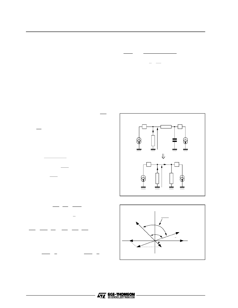
The dynamic representation of the output stage
can be depictedas below (Figure 22).
i
1
+
j
ω
R1 C1(at f = 500kHz)
R1 C1
ω
= 1
i
2
’ =
1
+
j
and Z = R1 +
j
ω
C<< R
i
≈
i
2
’
R1C1 network produces-45
o
phase lag of ”i” with
respect to ”i2”, around 500kHz.
V
18
≈
- R
(i
1
+ I
2
’)
i
1
andi
2
calculationas a functionof ”V
IN
” on Pin19
- A1 Amplifier :V
S1
with : I
2
’ =
i
2
1
V
IN
=R
C
dr
1
=1200
57= 21
dr : dynamicresistance =
λ
I
- A2 Amplifier:
i
2
V
S2
=
i
2
=0.39 V
IN
, i
2
is in phasewithV
IN
therefore :
i
3
= -i
2
= -0.39 V
IN
- A3 Amplifier:
i
1
= i
3
1
2dr
2
=1
54
i
2
V
IN
=
V
S1
V
IN
i
2
V
S1
= 0.395
V
C
A
λ
+
1
2
= - 0.39 V
IN
V
C
A
λ
+
1
2
17
18
1
i
2
i
V
18
R
i
18
C1
R1
17
18
1
i
V
18
R
i
18
i
Z
2
i ’
2
Figure 22
V
18
@ i
1
= 0
V
IN
V
OUT
phase variation = f(V
C
)
V
18
@ i
1 (Max.)
Ri
1
Ri
2
V
IN
-45
°
R (i + i )
2
R (i + i )
2
+136
°
2
Figure 23 :
VectorRepresentationof V
18
/V
IN
”V
IN
” always leads the ”i
1
” by 180, only the ampli-
tude of i
1
is a functionof V
C
(see Figure 23).
V
OUT
V
IN
1
+
j
(
R
1
+
R
)
C
1
ω
- i
1
= - 0.39 V
IN
-
= - R
i
1
(
1
+
j R
1
C
1
ω
)
+
i
2
i
2
V
C
4
λ
and i
2
= 0.39 V
IN
The Figure 24 illustrates the characteristics of
V
18
/V
IN
phaseversus V
C
.
- Phase variation determined by V
C
falls between
+24
o
and +135
o
range
- The gain is higher than 10dB. The Pin 18 output
signalof30to40dBhasarectangularcomponent
(see Figure 24).
TEA2028 - TEA2029 APPLICATIONNOTE
13/46
相關(guān)PDF資料 |
PDF描述 |
|---|---|
| TEA2028B | SWITCH MODE POWER SUPPLY PRIMARY CIRCUIT |
| TEA2128 | SWITCH MODE POWER SUPPLY PRIMARY CIRCUIT |
| TEA2164S | SWITCH MODE POWER SUPPLY PRIMARY CIRCUIT |
| TEA2029C | COLOR TV SCANNING AND POWER SUPPLY PROCESSOR |
| TEA2031A | COLOR TV EAST-WEST CORRECTION |
相關(guān)代理商/技術(shù)參數(shù) |
參數(shù)描述 |
|---|---|
| TEA2028B | 制造商:STMICROELECTRONICS 制造商全稱:STMicroelectronics 功能描述:COLOR TV SCANNING AND POWER SUPPLY PROCESSOR |
| TEA2028-TEA2029 | 制造商:STMICROELECTRONICS 制造商全稱:STMicroelectronics 功能描述:APPLICATION NOTE |
| TEA2029 | 制造商:STMICROELECTRONICS 制造商全稱:STMicroelectronics 功能描述:APPLICATION NOTE |
| TEA2029C | 制造商:STMICROELECTRONICS 制造商全稱:STMicroelectronics 功能描述:COLOR TV SCANNING AND POWER SUPPLY PROCESSOR |
| TEA2029CV | 制造商:TEMIC 制造商全稱:TEMIC Semiconductors 功能描述:Timing Processor (LINE, FRAME, SMPS) for TV Sets |
發(fā)布緊急采購,3分鐘左右您將得到回復(fù)。