- 您現(xiàn)在的位置:買賣IC網(wǎng) > PDF目錄361343 > T35L6464A (TM Technology, Inc.) 64K x 64 SRAM PDF資料下載
參數(shù)資料
| 型號: | T35L6464A |
| 廠商: | TM Technology, Inc. |
| 英文描述: | 64K x 64 SRAM |
| 中文描述: | 64K的× 64的SRAM |
| 文件頁數(shù): | 6/16頁 |
| 文件大?。?/td> | 160K |
| 代理商: | T35L6464A |

TE
CH
tm
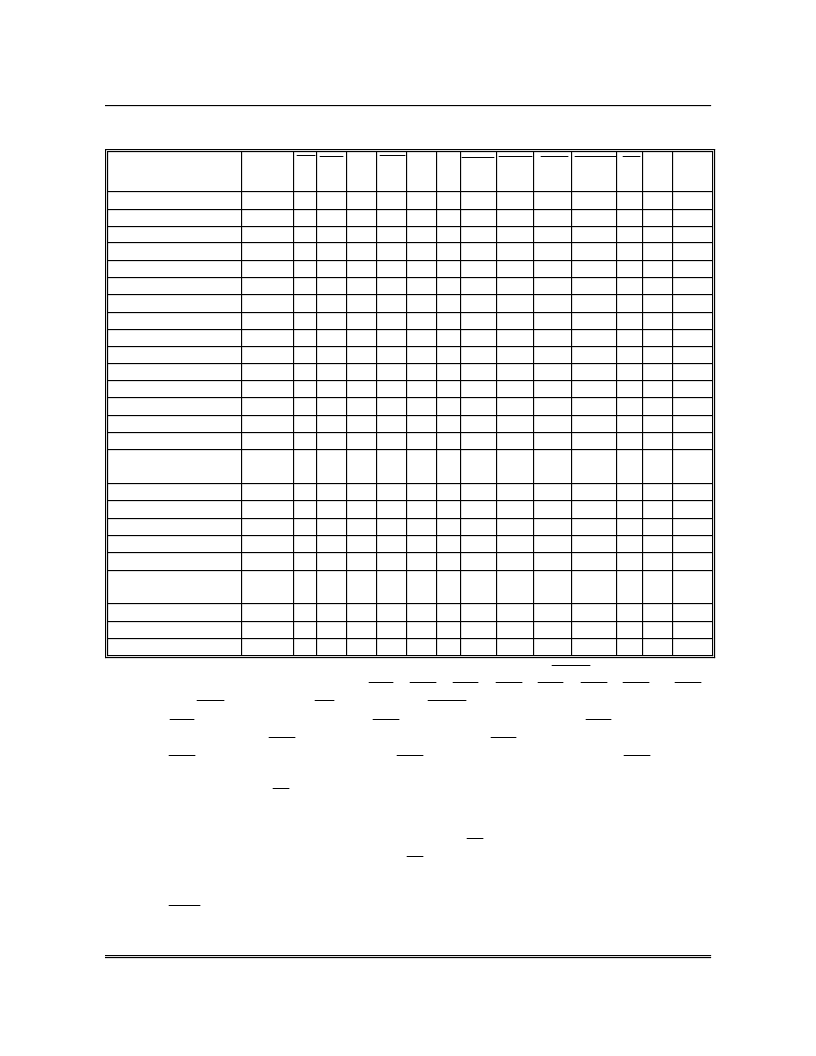
TRUTH TABLE
T35L6464A
Taiwan Memory Technology, Inc. reserves the right
P. 6
to change products or specifications without notice.
Publication Date: AUG. 1998
Revision: E
OPERATION
ADDRESS
USED
CE
CE2
CE2 CE3
CE3 ZZ
ADSP ADSC ADV WRITE
OE
CLK DQ
Deselected Cycle, Power Down
None
H
X
X
X
X
L
X
L
X
X
X
L-H
High-Z
Deselected Cycle, Power Down
None
L
X
X
X
L
L
L
X
X
X
X
L-H
High-Z
Deselected Cycle, Power Down
None
L
X
L
X
X
L
L
X
X
X
X
L-H
High-Z
Deselected Cycle, Power Down
None
L
X
X
H
X
L
L
X
X
X
X
L-H
High-Z
Deselected Cycle, Power Down
None
L
H
X
X
X
L
L
X
X
X
X
L-H
High-Z
Deselected Cycle, Power Down
None
L
X
X
X
L
L
H
L
X
X
X
L-H
High-Z
Deselected Cycle, Power Down
None
L
X
L
X
X
L
H
L
X
X
X
L-H
High-Z
Deselected Cycle, Power Down
Deselected Cycle, Power Down
None
None
L
L
X
H
X
X
H
X
X
X
L
L
H
H
L
L
X
X
X
X
X
X
L-H
L-H
High-Z
High-Z
Snooze Cycle, Power Down
None
X
X
X
X
X
H
X
X
X
X
X
X
High-Z
READ Cycle, Begin Burst
External
L
L
H
L
H
L
L
X
X
X
L
L-H
Q
READ Cycle, Begin Burst
External
L
L
H
L
H
L
L
X
X
X
H
L-H
High-Z
WRITE Cycle, Begin Burst
External
L
L
H
L
H
L
H
L
X
L
X
L-H
D
READ Cycle, Begin Burst
External
L
L
H
L
H
L
H
L
X
H
L
L-H
Q
READ Cycle, Begin Burst
READ Cycle, Continue Burst
External
Next
L
X
L
X
H
X
L
X
H
X
L
L
H
H
L
H
X
L
H
H
H
L
L-H
L-H
High-Z
Q
READ Cycle, Continue Burst
Next
X
X
X
X
X
L
H
H
L
H
H
L-H
High-Z
READ Cycle, Continue Burst
Next
H
X
X
X
X
L
X
H
L
H
L
L-H
Q
READ Cycle, Continue Burst
Next
H
X
X
X
X
L
X
H
L
H
H
L-H
High-Z
WRITE Cycle, Continue Burst
Next
X
X
X
X
X
L
H
H
L
L
X
L-H
D
WRITE Cycle, Continue Burst
Next
H
X
X
X
X
L
X
H
L
L
X
L-H
D
READ Cycle, Suspend Burst
Current
X
X
X
X
X
L
H
H
H
H
L
L-H
Q
READ Cycle, Suspend Burst
Current
X
X
X
X
X
L
H
H
H
H
H
L-H
High-Z
READ Cycle, Suspend Burst
Current
H
X
X
X
X
L
X
H
H
H
L
L-H
Q
READ Cycle, Suspend Burst
Current
H
X
X
X
X
L
X
H
H
H
H
L-H
High-Z
WRITE Cycle, Suspend Burst
Current
X
X
X
X
X
L
H
H
H
L
X
L-H
D
WRITE Cycle, Suspend Burst
Current
H
X
X
X
X
L
X
H
H
L
X
L-H
D
Note:
1. X means "don't care." H means logic HIGH. L means logic LOW.
WRITE
= L means any one
or more byte write enable signals
(
BW1
,
BW2
,
BW3
,
BW4
,
BW5
,
BW6
,
BW7
or
BW8
)
and
BWE
are LOW, or
GW
equals LOW.
WRITE
= H means all byte write signal are HIGH.
2.
BW1
= enables write to DQ1-DQ8.
BW2
= enables write to DQ9-DQ16.
BW3
= enables write
to DQ17-DQ24.
BW4
=enables write to DQ25-DQ32.
BW5
= enables write to DQ33-DQ40.
BW6
= enables write to DQ41-DQ48.
BW7
= enables write to DQ49-DQ56.
BW8
= enables
write to DQ57-DQ64.
3. All inputs except
OE
must meet setup and hold times around the rising edge ( LOW to HIGH)
of CLK.
4. Suspending burst generates wait cycle.
5. For a write operation following a read operation.
OE
must be HIGH before the input data
required setup time plus High-Z time for
OE
and staying HIGH throughout the input data hold
time.
6. This device contains circuitry that will ensure the outputs will be High-Z during power-up.
7.
ADSP
= LOW along with chip being selected always initiates an internal READ cycle at the L-H
edge of CLK. A WRITE cycle can be performed by setting WRITE LOW for the CLK L-H edge
of the subsequent wait cycle. Refer to WRITE timing diagram for clarification.
相關(guān)PDF資料 |
PDF描述 |
|---|---|
| T35L6464A-5L | 64K x 64 SRAM |
| T35L6464A-5Q | 64K x 64 SRAM |
| T3A6CIA | Bi-Directional Triode Thyristor Silicon Planar Type 3A Mold Triac(3A三端雙向可控硅開關(guān)元件) |
| T3A6CI | RECTIFIER STANDARD SINGLE 3A 400V 400 100A-ifsm 10uA-ir 1.15V-vf PowerDI?5 5K/REEL |
| T4312816A | 8M x 16 SDRAM |
相關(guān)代理商/技術(shù)參數(shù) |
參數(shù)描述 |
|---|---|
| T35L6464A-5L | 制造商:TMT 制造商全稱:TMT 功能描述:64K x 64 SRAM |
| T35L6464A-5Q | 制造商:TMT 制造商全稱:TMT 功能描述:64K x 64 SRAM |
| T-35SP | 制造商:Triad Magnetics 功能描述: |
| T-35X | 制造商:Triad Magnetics 功能描述: |
| T36 | 制造商:MELCO 功能描述:MELCO TOMMY BAR T36 5/16"DIA |
發(fā)布緊急采購,3分鐘左右您將得到回復(fù)。