- 您現(xiàn)在的位置:買賣IC網(wǎng) > PDF目錄358393 > SIHFP260-E3 (VISHAY SILICONIX) 46 A, 200 V, 0.055 ohm, N-CHANNEL, Si, POWER, MOSFET, TO-247 PDF資料下載
參數(shù)資料
| 型號(hào): | SIHFP260-E3 |
| 廠商: | VISHAY SILICONIX |
| 元件分類: | JFETs |
| 英文描述: | 46 A, 200 V, 0.055 ohm, N-CHANNEL, Si, POWER, MOSFET, TO-247 |
| 封裝: | ROHS COMPLIANT PACKAGE-3 |
| 文件頁數(shù): | 2/9頁 |
| 文件大小: | 1762K |
| 代理商: | SIHFP260-E3 |
www.vishay.com
2
Document Number: 91215
S11-0487-Rev. B, 21-Mar-11
This datasheet is subject to change without notice.
THE PRODUCT DESCRIBED HEREIN AND THIS DATASHEET ARE SUBJECT TO SPECIFIC DISCLAIMERS, SET FORTH AT
www.vishay.com/doc91000
IRFP260, SiHFP260
Vishay Siliconix
Notes
a. Repetitive rating; pulse width limited by maximum junction temperature (see fig. 11).
b. Pulse width
≤
300 μs; duty cycle
≤
2 %.
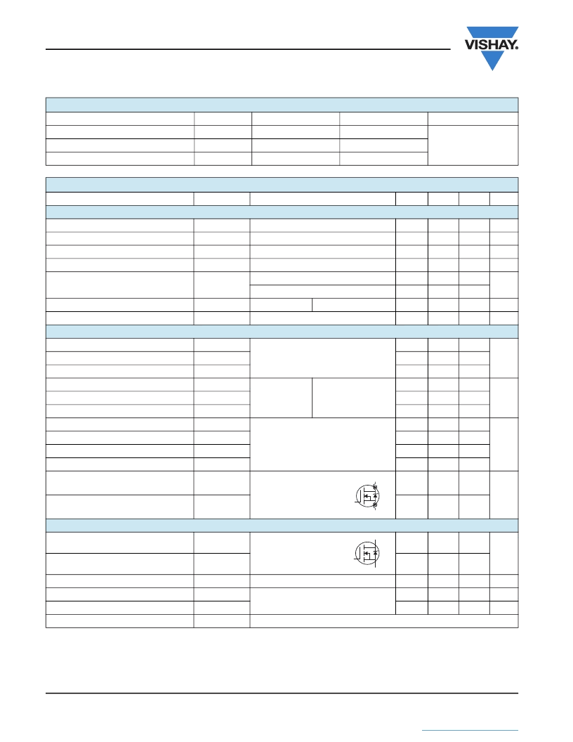
THERMAL RESISTANCE RATINGS
PARAMETER
SYMBOL
TYP.
MAX.
UNIT
Maximum Junction-to-Ambient
R
thJA
R
thCS
R
thJC
-
40
°C/W
Case-to-Sink, Flat, Greased Surface
0.24
-
Maximum Junction-to-Case (Drain)
-
0.45
SPECIFICATIONS
(T
J
= 25 °C, unless otherwise noted)
PARAMETER
SYMBOL
TEST CONDITIONS
MIN.
TYP.
MAX.
UNIT
Static
Drain-Source Breakdown Voltage
V
DS
V
GS
= 0 V, I
D
= 250 μA
Reference to 25 °C, I
D
= 1 mA
V
DS
= V
GS
, I
D
= 250 μA
V
GS
= ± 20 V
V
DS
= 200 V, V
GS
= 0 V
V
DS
= 160 V, V
GS
= 0 V, T
J
= 125 °C
V
GS
= 10 V
V
DS
= 50 V, I
D
= 28 A
b
200
-
-
V
V
DS
Temperature Coefficient
Gate-Source Threshold Voltage
Δ
V
DS
/T
J
V
GS(th)
I
GSS
-
0.24
-
V/°C
2.0
-
4.0
V
nA
Gate-Source Leakage
-
-
± 100
Zero Gate Voltage Drain Current
I
DSS
-
-
25
μA
-
-
250
Drain-Source On-State Resistance
R
DS(on)
g
fs
I
D
= 28 A
b
-
-
0.055
Ω
Forward Transconductance
24
-
-
S
Dynamic
Input Capacitance
C
iss
C
oss
C
rss
Q
g
Q
gs
Q
gd
t
d(on)
t
r
t
d(off)
t
f
V
GS
= 0 V,
V
DS
= 25 V,
f = 1.0 MHz, see fig. 5
-
5200
-
pF
Output Capacitance
-
1200
-
Reverse Transfer Capacitance
-
310
-
Total Gate Charge
V
GS
= 10 V
I
D
= 46 A, V
= 160 V,
see fig. 6 and 13
b
-
-
230
nC
Gate-Source Charge
-
-
42
Gate-Drain Charge
-
-
110
Turn-On Delay Time
V
DD
= 100 V, I
D
= 46 A,
R
g
= 4.3
Ω
, R
D
= 2.1
Ω
, see fig. 10
b
-
23
-
ns
Rise Time
-
120
-
Turn-Off Delay Time
-
100
-
Fall Time
-
94
-
Internal Drain Inductance
L
D
Between lead,
6 mm (0.25") from
package and center of
die contact
-
5.0
-
nH
Internal Source Inductance
L
S
-
13
-
Drain-Source Body Diode Characteristics
Continuous Source-Drain Diode Current
I
S
MOSFET symbol
showing the
integral reverse
p - n junction diode
-
-
46
A
Pulsed Diode Forward Current
a
I
SM
-
-
180
Body Diode Voltage
V
SD
t
rr
Q
rr
t
on
T
J
= 25 °C, I
S
= 46 A, V
GS
= 0 V
b
-
-
1.8
V
Body Diode Reverse Recovery Time
T
J
= 25 °C, I
F
= 46 A, dI/dt = 100 A/μs
b
-
390
590
ns
Body Diode Reverse Recovery Charge
-
4.8
7.2
μC
Forward Turn-On Time
Intrinsic turn-on time is negligible (turn-on is dominated by L
S
and L
D
)
D
S
G
S
D
G
相關(guān)PDF資料 |
PDF描述 |
|---|---|
| SIHFR120T | 7.7 A, 100 V, 0.27 ohm, N-CHANNEL, Si, POWER, MOSFET, TO-252AA |
| SIHFR320-E3 | 3.1 A, 400 V, 1.8 ohm, N-CHANNEL, Si, POWER, MOSFET, TO-252 |
| SIHFZ48 | 50 A, 60 V, 0.018 ohm, N-CHANNEL, Si, POWER, MOSFET, TO-220AB |
| SIHL540STL | 28 A, 100 V, 0.077 ohm, N-CHANNEL, Si, POWER, MOSFET, TO-263AB |
| SIL03-1A72-71M | DRY REED RELAY, SPST, MOMENTARY, 0.006A (COIL), 3VDC (COIL), 18mW (COIL), 0.5A (CONTACT), 200VDC (CONTACT), THROUGH HOLE-STRAIGHT MOUNT |
相關(guān)代理商/技術(shù)參數(shù) |
參數(shù)描述 |
|---|---|
| SIHFP264 | 制造商:VISHAY 制造商全稱:Vishay Siliconix 功能描述:Power MOSFET |
| SIHFP264-E3 | 制造商:VISHAY 制造商全稱:Vishay Siliconix 功能描述:Power MOSFET |
| SIHFP264N | 制造商:VISHAY 制造商全稱:Vishay Siliconix 功能描述:Power MOSFET |
| SIHFP264N-E3 | 制造商:VISHAY 制造商全稱:Vishay Siliconix 功能描述:Power MOSFET |
| SIHFP26N60L | 制造商:VISHAY 制造商全稱:Vishay Siliconix 功能描述:Power MOSFET |
發(fā)布緊急采購,3分鐘左右您將得到回復(fù)。