- 您現(xiàn)在的位置:買賣IC網(wǎng) > PDF目錄296941 > QL6250E-8PS484M (QUICKLOGIC CORP) FPGA, 960 CLBS, 248160 GATES, PBGA484 PDF資料下載
參數(shù)資料
| 型號: | QL6250E-8PS484M |
| 廠商: | QUICKLOGIC CORP |
| 元件分類: | FPGA |
| 英文描述: | FPGA, 960 CLBS, 248160 GATES, PBGA484 |
| 封裝: | 23 X 23 MM, 1 MM PITCH, MS-034AAJ-1, PLASTIC, BGA-484 |
| 文件頁數(shù): | 36/64頁 |
| 文件大小: | 850K |
| 代理商: | QL6250E-8PS484M |
第1頁第2頁第3頁第4頁第5頁第6頁第7頁第8頁第9頁第10頁第11頁第12頁第13頁第14頁第15頁第16頁第17頁第18頁第19頁第20頁第21頁第22頁第23頁第24頁第25頁第26頁第27頁第28頁第29頁第30頁第31頁第32頁第33頁第34頁第35頁當(dāng)前第36頁第37頁第38頁第39頁第40頁第41頁第42頁第43頁第44頁第45頁第46頁第47頁第48頁第49頁第50頁第51頁第52頁第53頁第54頁第55頁第56頁第57頁第58頁第59頁第60頁第61頁第62頁第63頁第64頁
2006 QuickLogic Corporation
Eclipse-E Family Data Sheet Rev. A
41
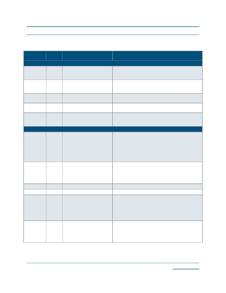
PT280 and PS484 Pin Descriptions
Table 26: PT280 and PS484 Pin Descriptions
Pin
Directio
n
Function
Description
JTAG Pin Descriptions
TDI/RSI
I
Test Data In for JTAG/RAM init.
Serial Data In
Hold HIGH during normal operation. Connects to serial
PROM data in for RAM initialization. Connect to VDED2 if
unused
TRSTB/RRO
I/0
Active low Reset for JTAG/RAM
init. reset out
Hold LOW during normal operation. Connects to serial
PROM reset for RAM initialization. Connect to GND if
unused
TMS
I
Test Mode Select for JTAG
Hold HIGH during normal operation. Connect to VDED2 if
not used for JTAG
TCK
I
Test Clock for JTAG
Hold HIGH or LOW during normal operation. Connect to
VDED2 or GND if not used for JTAG
TDO/RCO
O
Test data out for JTAG/RAM init.
clock out
Connect to serial PROM clock for RAM initialization. Must be
left unconnected if not used for JTAG or RAM initialization.
The output voltage drive is specified by VCCIO(C).
Dedicated Pin Descriptions
CLK
I
Global clock network pin
Low skew global clock. This pin provides access to a
dedicated, distributed network capable of driving the
CLOCK, SET, RESET, F1, and A2 inputs to the Logic Cell,
READ, and WRITE CLOCKS, Read and Write Enables of
the Embedded RAM Blocks, CLOCK of the ECUs, and
Output Enables of the I/Os. The voltage tolerance of this pin
is specified by VCCIO(C).
DEDCLK
I
Dedicated clock pin
Very low skew global clock. This pin provides access to a
dedicated, distributed clock network capable of driving the
CLOCK inputs of all sequential elements of the device (e.g.,
RAM, Flip Flops). The voltage tolerance of this pin is
specified by VCCIO(C).
GND
I
Ground pin
Connect to ground.
GNDPLL
I
Ground pin for PLL
Connect to GND.
INREF(A)
I
Differential reference voltage
The INREF is the reference voltage pin for GTL+, SSTL2,
and STTL3 standards. Follow the recommendations
provided in
Table 13 for the appropriate standard. The A
inside the parenthesis means that INREF is located in BANK
A. This pin should be tied to GND if voltage referenced
standards are not used.
I/O(A)
I/O
Input/Output pin
The I/O pin is a bi-directional pin, configurable to either an
input-only, output-only, or bi-directional pin. The A inside the
parenthesis means that the I/O is located in Bank A. If an I/O
is not used, SpDE (QuickWorks Tool) provides the option of
tying that pin to GND, VCC
, or TriState.
相關(guān)PDF資料 |
PDF描述 |
|---|---|
| QL6325-4PB516C | FPGA, 1536 CLBS, 320640 GATES, PBGA516 |
| QL8150-6PTN196M | FPGA, 640 CLBS, 188946 GATES, PBGA196 |
| QL8150-8PTN196C | FPGA, 640 CLBS, 188946 GATES, PBGA196 |
| QL8150-8PTN196I | FPGA, 640 CLBS, 188946 GATES, PBGA196 |
| QL8150-6PFN144C | FPGA, 640 CLBS, 188946 GATES, PQFP144 |
相關(guān)代理商/技術(shù)參數(shù) |
參數(shù)描述 |
|---|---|
| QL6325PQ208 | 制造商:未知廠家 制造商全稱:未知廠家 功能描述:ASIC |
| QL6325PT280 | 制造商:未知廠家 制造商全稱:未知廠家 功能描述:ASIC |
| QL63D5SA | 制造商:未知廠家 制造商全稱:未知廠家 功能描述:InGaAlP Laser Diode |
| QL63F5SA | 制造商:未知廠家 制造商全稱:未知廠家 功能描述:InGaAlP Laser Diode |
| QL63H5S-A | 制造商:ROITHNER 制造商全稱:ROITHNER 功能描述:INGaAIP Laser Diode |
發(fā)布緊急采購,3分鐘左右您將得到回復(fù)。