- 您現(xiàn)在的位置:買賣IC網(wǎng) > PDF目錄296941 > QL6250E-8PS484M (QUICKLOGIC CORP) FPGA, 960 CLBS, 248160 GATES, PBGA484 PDF資料下載
參數(shù)資料
| 型號: | QL6250E-8PS484M |
| 廠商: | QUICKLOGIC CORP |
| 元件分類: | FPGA |
| 英文描述: | FPGA, 960 CLBS, 248160 GATES, PBGA484 |
| 封裝: | 23 X 23 MM, 1 MM PITCH, MS-034AAJ-1, PLASTIC, BGA-484 |
| 文件頁數(shù): | 34/64頁 |
| 文件大小: | 850K |
| 代理商: | QL6250E-8PS484M |
第1頁第2頁第3頁第4頁第5頁第6頁第7頁第8頁第9頁第10頁第11頁第12頁第13頁第14頁第15頁第16頁第17頁第18頁第19頁第20頁第21頁第22頁第23頁第24頁第25頁第26頁第27頁第28頁第29頁第30頁第31頁第32頁第33頁當(dāng)前第34頁第35頁第36頁第37頁第38頁第39頁第40頁第41頁第42頁第43頁第44頁第45頁第46頁第47頁第48頁第49頁第50頁第51頁第52頁第53頁第54頁第55頁第56頁第57頁第58頁第59頁第60頁第61頁第62頁第63頁第64頁
2006 QuickLogic Corporation
Eclipse-E Family Data Sheet Rev. A
4
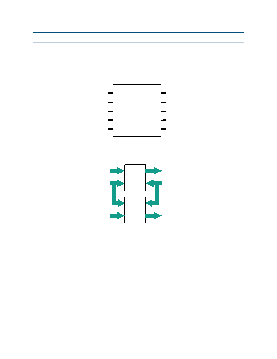
RAM Modules
The Eclipse-E family includes up to 24 dual-port 2,304-bit RAM modules for implementing RAM, ROM, and
FIFO functions. Each module is user-configurable into four different block organizations and can be cascaded
horizontally to increase their effective width, or vertically to increase their effective depth as shown in Figure 4.
Figure 3: 2,304-bit RAM Module
Using the two “mode” pins, designers can configure each module into 128 x 18 and 256 x 9. The blocks are
also easily cascadable to increase their effective width and/or depth (see Figure 4
).
Figure 4: Cascaded RAM Modules
The RAM modules are dual-port, with completely independent READ and WRITE ports and separate READ
and WRITE clocks. The READ ports support asynchronous and synchronous operation, while the WRITE
ports support synchronous operation. Each port has 18 data lines and 8 address lines, allowing word lengths
of up to 18 bits and address spaces of up to 256 words. Depending on the mode selected, however, some
higher order data or address lines may not be used.
The Write Enable (WE) line acts as a clock enable for synchronous write operation. The Read Enable (RE) acts
as a clock enable for synchronous READ operation (ASYNCRD input low), or as a flow-through enable for
asynchronous READ operation (ASYNCRD input high).
Designers can cascade multiple RAM modules to increase the depth or width allowed in single modules by
connecting corresponding address lines together and dividing the words between modules.
A similar technique can be used to create depths greater than 256 words. In this case address signals higher
than the MSB are encoded onto the write enable (WE) input for WRITE operations. The READ data outputs
are multiplexed together using encoded higher READ address bits for the multiplexer SELECT signals.
The RAM blocks can be loaded with data generated internally (typically for RAM or FIFO functions) or with
data from an external PROM (typically for ROM functions).
MODE[1:0]
WA[9:0]
WD[17:0]
WE
WCLK
ASYNCRD
RA[9:0]
RD[17:0]
RE
RCLK
WDATA
RDATA
WADDR
WDATA
RADDR
RAM
Module
(2,304 bits)
RAM
Module
(2,304 bits)
相關(guān)PDF資料 |
PDF描述 |
|---|---|
| QL6325-4PB516C | FPGA, 1536 CLBS, 320640 GATES, PBGA516 |
| QL8150-6PTN196M | FPGA, 640 CLBS, 188946 GATES, PBGA196 |
| QL8150-8PTN196C | FPGA, 640 CLBS, 188946 GATES, PBGA196 |
| QL8150-8PTN196I | FPGA, 640 CLBS, 188946 GATES, PBGA196 |
| QL8150-6PFN144C | FPGA, 640 CLBS, 188946 GATES, PQFP144 |
相關(guān)代理商/技術(shù)參數(shù) |
參數(shù)描述 |
|---|---|
| QL6325PQ208 | 制造商:未知廠家 制造商全稱:未知廠家 功能描述:ASIC |
| QL6325PT280 | 制造商:未知廠家 制造商全稱:未知廠家 功能描述:ASIC |
| QL63D5SA | 制造商:未知廠家 制造商全稱:未知廠家 功能描述:InGaAlP Laser Diode |
| QL63F5SA | 制造商:未知廠家 制造商全稱:未知廠家 功能描述:InGaAlP Laser Diode |
| QL63H5S-A | 制造商:ROITHNER 制造商全稱:ROITHNER 功能描述:INGaAIP Laser Diode |
發(fā)布緊急采購,3分鐘左右您將得到回復(fù)。