- 您現(xiàn)在的位置:買賣IC網(wǎng) > PDF目錄69257 > PTPS65910A1RSL (TEXAS INSTRUMENTS INC) POWER SUPPLY SUPPORT CKT, PQCC48 PDF資料下載
參數(shù)資料
| 型號(hào): | PTPS65910A1RSL |
| 廠商: | TEXAS INSTRUMENTS INC |
| 元件分類: | 電源管理 |
| 英文描述: | POWER SUPPLY SUPPORT CKT, PQCC48 |
| 封裝: | 6 X 6 MM, 1 MM HEIGHT, GREEN, PLASTIC,VQFN-48 |
| 文件頁(yè)數(shù): | 27/89頁(yè) |
| 文件大小: | 941K |
| 代理商: | PTPS65910A1RSL |
第1頁(yè)第2頁(yè)第3頁(yè)第4頁(yè)第5頁(yè)第6頁(yè)第7頁(yè)第8頁(yè)第9頁(yè)第10頁(yè)第11頁(yè)第12頁(yè)第13頁(yè)第14頁(yè)第15頁(yè)第16頁(yè)第17頁(yè)第18頁(yè)第19頁(yè)第20頁(yè)第21頁(yè)第22頁(yè)第23頁(yè)第24頁(yè)第25頁(yè)第26頁(yè)當(dāng)前第27頁(yè)第28頁(yè)第29頁(yè)第30頁(yè)第31頁(yè)第32頁(yè)第33頁(yè)第34頁(yè)第35頁(yè)第36頁(yè)第37頁(yè)第38頁(yè)第39頁(yè)第40頁(yè)第41頁(yè)第42頁(yè)第43頁(yè)第44頁(yè)第45頁(yè)第46頁(yè)第47頁(yè)第48頁(yè)第49頁(yè)第50頁(yè)第51頁(yè)第52頁(yè)第53頁(yè)第54頁(yè)第55頁(yè)第56頁(yè)第57頁(yè)第58頁(yè)第59頁(yè)第60頁(yè)第61頁(yè)第62頁(yè)第63頁(yè)第64頁(yè)第65頁(yè)第66頁(yè)第67頁(yè)第68頁(yè)第69頁(yè)第70頁(yè)第71頁(yè)第72頁(yè)第73頁(yè)第74頁(yè)第75頁(yè)第76頁(yè)第77頁(yè)第78頁(yè)第79頁(yè)第80頁(yè)第81頁(yè)第82頁(yè)第83頁(yè)第84頁(yè)第85頁(yè)第86頁(yè)第87頁(yè)第88頁(yè)第89頁(yè)
PRODUCTPREVIEW
SWCS046-022
VCC7
VIO
INT1
1.8V
Td32KON
NRESPWON
TdSONT
Switch On sequence
Intterupt aknowledge
PWRHOLD
VMBHI_IT=1
TdONVMBHI
CLK33KOUT
VMBCH threshold
VMBHI threshold
VRTC
1.8V
TdbVMBHI
VMBDCH threshold
VMBLO threshold
VBNPR threshold
TdbVMBDCH
TdbVMBLO
Switch Off sequence
VBACKUP > VBNPR
www.ti.com
SWCS046C – MARCH 2010 – REVISED JUNE 2010
POWER CONTROL TIMING (continued)
Table 6. Power Control Timing Characteristics
PARAMETER
TEST CONDITIONS
MIN
TYP
MAX
UNIT
tdbPWRONF: PWRON falling-edge debouncing delay
500
550
s
3 ×
4 ×
tdbPWRONR: PWRON rising-edge debouncing delay
tCK32k
tCK32k =
s
= 94
125
2 ×
3 ×
tdbPWRHOLD: PWRON rising-edge debouncing delay
tCK32k
tCK32k=
s
= 63
94
tdOINT: INT1 (internal) Power-on pulse duration after
1
s
PWRON low-level (debounced) event
tdONPWHOLD: delay to set high PWRHOLD signal or
DEV_ON control bit after NRESPWON released to
984
ms
keep on the supplies
tdPWRONLP: PWRON long-press delay (disabling
PWON falling edge to
6
s
power-on condition) to INT1 falling edge
INT1 falling edge
tdPWRONLPTO: PWROW long-press interrupt
INT1 falling edge to
2
s
(PWRON_LP_IT) to supplies switch-off
NRESPWON falling edge
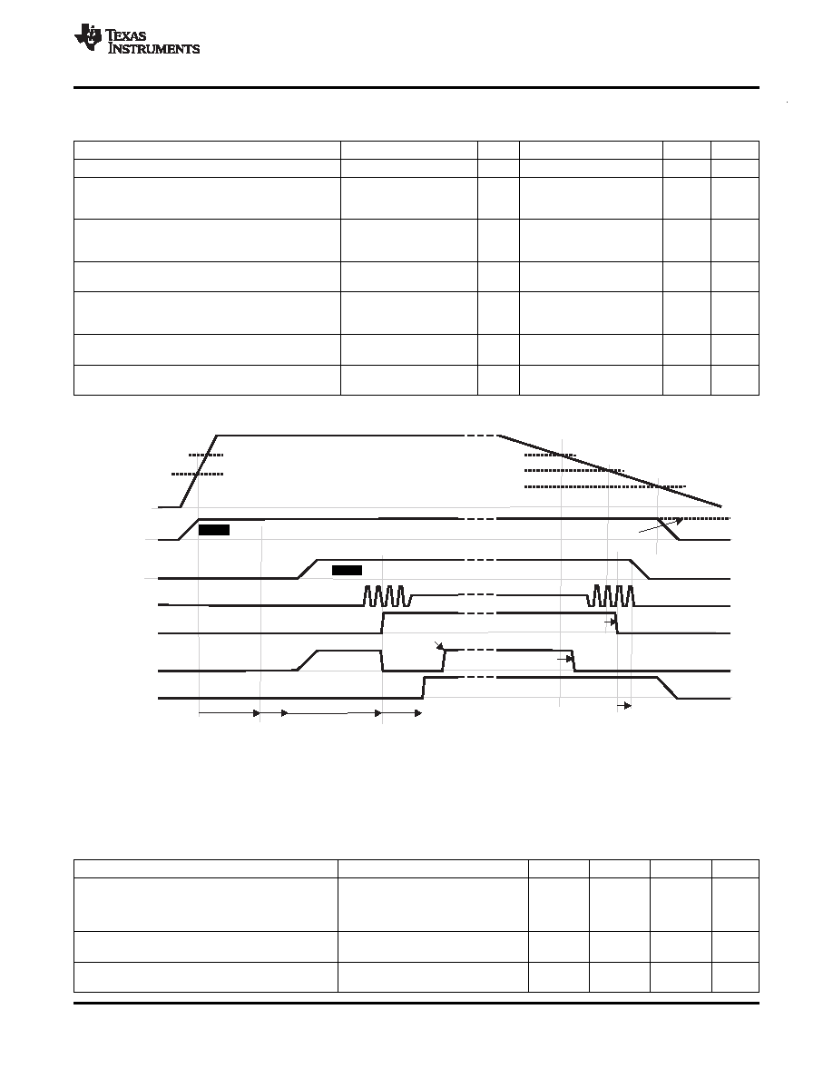
Device turn-on with rising input voltage
Figure 6. Device Turn-On/Off with Rising/Falling Input Voltage
Note: The DEV_ON control bit can be used instead of the PWRHOLD signal to maintain supplies on after the
switch-on sequence.
Table 7. Device Turn-on/off with Rising/Falling Input Voltage, Timing Characteristics
PARAMETER
TEST CONDITIONS
MIN
TYP
MAX
UNIT
BOOT[1:0] = 00, RC oscillator
0.1
td32KON: 32-kHz oscillator turn on time
BOOT[1:0] = 01, quartz oscillator
200
ms
BOOT[1:0] = 01, bypass clock
0.1
3 × tCK32k
4 × tCK32k
tdbVMBHI: VMBHI rising-edge debouncing delay
s
= 94
= 125
tdOINT: INT1 Power On pulse duration after VMBHI
1
s
high-level (debounced) event
Copyright 2010, Texas Instruments Incorporated
33
相關(guān)PDF資料 |
PDF描述 |
|---|---|
| PTPS659106A1RSLR | POWER SUPPLY SUPPORT CKT, PQCC48 |
| PTPS659102A1RSLR | POWER SUPPLY SUPPORT CKT, PQCC48 |
| PTPS659104A1RSLR | POWER SUPPLY SUPPORT CKT, PQCC48 |
| PTPS659107A1RSL | POWER SUPPLY SUPPORT CKT, PQCC48 |
| PTPS659105A1RSLR | POWER SUPPLY SUPPORT CKT, PQCC48 |
相關(guān)代理商/技術(shù)參數(shù) |
參數(shù)描述 |
|---|---|
| PTPS6591102A2ZRCR | 制造商:TI 功能描述:TPS65911 |
| PTPS6591102ZRC | 制造商:TI 功能描述:TPS65911 |
| PTPS6591104A2ZRCR | 制造商:TI 功能描述:TPS65911 |
| PTPS659110A2ZRC | 制造商:TI 功能描述:TPS65911 |
| PTPS659110A2ZRCR | 制造商:TI 功能描述:TPS65911 |
發(fā)布緊急采購(gòu),3分鐘左右您將得到回復(fù)。