- 您現(xiàn)在的位置:買賣IC網(wǎng) > PDF目錄368224 > PSD4235G2 Flash In-System-Programmable Peripherals for 16-Bit MCUs(用于16位MCU的閃速在系統(tǒng)可編程外圍芯片) PDF資料下載
參數(shù)資料
| 型號: | PSD4235G2 |
| 英文描述: | Flash In-System-Programmable Peripherals for 16-Bit MCUs(用于16位MCU的閃速在系統(tǒng)可編程外圍芯片) |
| 中文描述: | Flash在系統(tǒng)可編程外設(shè)的16位微控制器(用于16位微控制器的閃速在系統(tǒng)可編程外圍芯片) |
| 文件頁數(shù): | 74/114頁 |
| 文件大?。?/td> | 567K |
| 代理商: | PSD4235G2 |
第1頁第2頁第3頁第4頁第5頁第6頁第7頁第8頁第9頁第10頁第11頁第12頁第13頁第14頁第15頁第16頁第17頁第18頁第19頁第20頁第21頁第22頁第23頁第24頁第25頁第26頁第27頁第28頁第29頁第30頁第31頁第32頁第33頁第34頁第35頁第36頁第37頁第38頁第39頁第40頁第41頁第42頁第43頁第44頁第45頁第46頁第47頁第48頁第49頁第50頁第51頁第52頁第53頁第54頁第55頁第56頁第57頁第58頁第59頁第60頁第61頁第62頁第63頁第64頁第65頁第66頁第67頁第68頁第69頁第70頁第71頁第72頁第73頁當(dāng)前第74頁第75頁第76頁第77頁第78頁第79頁第80頁第81頁第82頁第83頁第84頁第85頁第86頁第87頁第88頁第89頁第90頁第91頁第92頁第93頁第94頁第95頁第96頁第97頁第98頁第99頁第100頁第101頁第102頁第103頁第104頁第105頁第106頁第107頁第108頁第109頁第110頁第111頁第112頁第113頁第114頁
PSD4000 Series
Beta Information
70
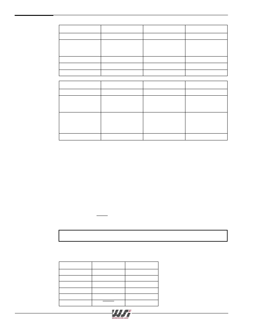
Port E Pin
PE0
PE1
PE2
PE3
PE4
PE5
JTAG Signals
TMS
TCK
TDI
TDO
TSTAT
TERR
Description
Mode Select
Clock
Serial Data In
Serial Data Out
Status
Error Flag
Table 33. JTAG Port Signals
The
PSD4000
Functional
Blocks
(cont.)
9.6 Programming In-Circuit using the JTAG-ISP Interface
The JTAG-ISP interface on the PSD4000 can be enabled on Port E (see Table 33). All
memory (Flash and Flash Boot Block), PLD logic, and PSD configuration bits may be
programmed through the JTAG-ISC interface. A blank part can be mounted on a printed
circuit board and programmed using JTAG-ISP.
The standard JTAG signals (IEEE 1149.1) are TMS, TCK, TDI, and TDO. Two additional
signals, TSTAT and TERR, are optional JTAG extensions used to speed up program and
erase operations.
*
SR_cod and Periph Mode bits in the VM Register are always cleared to zero on power on or warm reset.
**
9.5.3.4 Reset of Flash Erase and Programming Cycles
An external reset on the RESET pin will also reset the internal Flash memory state
machine. When the Flash is in programming or erase mode, the RESET pin will terminate
the programming or erase operation and return the Flash back to read mode in tNLNH-A
(minimum 25 μs) time.
Port Configuration
MCU I/O
PLD Output
Power On Reset
Input Mode
Valid after internal
PSD configuration
bits are loaded
Tri-stated
Tri-stated
Tri-stated
Warm Reset
Input Mode
Valid
Power Down Mode
Unchanged
Depend on inputs to
PLD (address are
blocked in PD mode)
Not defined
Tri-stated
Tri-stated
Address Out
Data Port
Peripheral I/O
Tri-stated
Tri-stated
Tri-stated
Table 32. Status During Power On Reset, Warm Reset and Power Down Mode
Register
Power On Reset
Cleared to
“
0
”
Cleared to
“
0
”
by
internal power on
reset
Initialized based on
the selection in
PSDsoft
Configuration Menu.
Cleared to
“
0
”
Warm Reset
Unchanged
Depend on .re and
.pr equations
Power Down Mode
Unchanged
Depend on .re and
.pr equations
PMMR0, 2
Micro
Cells Flip
Flop status
VM Register*
Initialized based on
the selection in
PSDsoft
Configuration Menu.
Cleared to
“
0
”
Unchanged
All other registers
Unchanged
By default, on a blank PSD (as shipped from factory or after erasure), four pins on Port E
are enabled for the basic JTAG signals TMS, TCK, TDI, and TDO.
See Waferscale Application Note 54 for more details on JTAG In-System-Programming.
相關(guān)PDF資料 |
PDF描述 |
|---|---|
| PSD4235G2 | FLASH IN-SYSTEM PROGRAMMABLE (ISP) PERIPHERALS FOR 16-BIT MCUS (5V SUPPLY) |
| PSD4235G2V | -200V 100kRad Hi-Rel Single P-Channel TID Hardened MOSFET in a TO-254AA package; A JANSR2N7426 with Standard Packaging |
| PSD4235G1-B-12J | Flash In-System Programmable ISP Peripherals For 16-bit MCUs 5V Supply |
| PSD4235F2-A-12J | Flash In-System Programmable ISP Peripherals For 16-bit MCUs 5V Supply |
| PSD4235G2-A-12J | Flash In-System Programmable ISP Peripherals For 16-bit MCUs 5V Supply |
相關(guān)代理商/技術(shù)參數(shù) |
參數(shù)描述 |
|---|---|
| PSD4235G2-70U | 功能描述:SPLD - 簡單可編程邏輯器件 5.0V 4M 70ns RoHS:否 制造商:Texas Instruments 邏輯系列:TICPAL22V10Z 大電池?cái)?shù)量:10 最大工作頻率:66 MHz 延遲時(shí)間:25 ns 工作電源電壓:4.75 V to 5.25 V 電源電流:100 uA 最大工作溫度:+ 75 C 最小工作溫度:0 C 安裝風(fēng)格:Through Hole 封裝 / 箱體:DIP-24 |
| PSD4235G2-90U | 功能描述:CPLD - 復(fù)雜可編程邏輯器件 5.0V 4M 90ns RoHS:否 制造商:Lattice 系列: 存儲類型:EEPROM 大電池?cái)?shù)量:128 最大工作頻率:333 MHz 延遲時(shí)間:2.7 ns 可編程輸入/輸出端數(shù)量:64 工作電源電壓:3.3 V 最大工作溫度:+ 90 C 最小工作溫度:0 C 封裝 / 箱體:TQFP-100 |
| PSD4235G2-90UI | 功能描述:CPLD - 復(fù)雜可編程邏輯器件 5.0V 4M 90ns RoHS:否 制造商:Lattice 系列: 存儲類型:EEPROM 大電池?cái)?shù)量:128 最大工作頻率:333 MHz 延遲時(shí)間:2.7 ns 可編程輸入/輸出端數(shù)量:64 工作電源電壓:3.3 V 最大工作溫度:+ 90 C 最小工作溫度:0 C 封裝 / 箱體:TQFP-100 |
| PSD4235G2V-12UI | 功能描述:CPLD - 復(fù)雜可編程邏輯器件 3.3V 4M 120ns RoHS:否 制造商:Lattice 系列: 存儲類型:EEPROM 大電池?cái)?shù)量:128 最大工作頻率:333 MHz 延遲時(shí)間:2.7 ns 可編程輸入/輸出端數(shù)量:64 工作電源電壓:3.3 V 最大工作溫度:+ 90 C 最小工作溫度:0 C 封裝 / 箱體:TQFP-100 |
| PSD4235G2V-90U | 功能描述:CPLD - 復(fù)雜可編程邏輯器件 3.3V 4M 90ns RoHS:否 制造商:Lattice 系列: 存儲類型:EEPROM 大電池?cái)?shù)量:128 最大工作頻率:333 MHz 延遲時(shí)間:2.7 ns 可編程輸入/輸出端數(shù)量:64 工作電源電壓:3.3 V 最大工作溫度:+ 90 C 最小工作溫度:0 C 封裝 / 箱體:TQFP-100 |
發(fā)布緊急采購,3分鐘左右您將得到回復(fù)。