- 您現(xiàn)在的位置:買賣IC網(wǎng) > PDF目錄368224 > PSD4235G2 Flash In-System-Programmable Peripherals for 16-Bit MCUs(用于16位MCU的閃速在系統(tǒng)可編程外圍芯片) PDF資料下載
參數(shù)資料
| 型號(hào): | PSD4235G2 |
| 英文描述: | Flash In-System-Programmable Peripherals for 16-Bit MCUs(用于16位MCU的閃速在系統(tǒng)可編程外圍芯片) |
| 中文描述: | Flash在系統(tǒng)可編程外設(shè)的16位微控制器(用于16位微控制器的閃速在系統(tǒng)可編程外圍芯片) |
| 文件頁(yè)數(shù): | 60/114頁(yè) |
| 文件大小: | 567K |
| 代理商: | PSD4235G2 |
第1頁(yè)第2頁(yè)第3頁(yè)第4頁(yè)第5頁(yè)第6頁(yè)第7頁(yè)第8頁(yè)第9頁(yè)第10頁(yè)第11頁(yè)第12頁(yè)第13頁(yè)第14頁(yè)第15頁(yè)第16頁(yè)第17頁(yè)第18頁(yè)第19頁(yè)第20頁(yè)第21頁(yè)第22頁(yè)第23頁(yè)第24頁(yè)第25頁(yè)第26頁(yè)第27頁(yè)第28頁(yè)第29頁(yè)第30頁(yè)第31頁(yè)第32頁(yè)第33頁(yè)第34頁(yè)第35頁(yè)第36頁(yè)第37頁(yè)第38頁(yè)第39頁(yè)第40頁(yè)第41頁(yè)第42頁(yè)第43頁(yè)第44頁(yè)第45頁(yè)第46頁(yè)第47頁(yè)第48頁(yè)第49頁(yè)第50頁(yè)第51頁(yè)第52頁(yè)第53頁(yè)第54頁(yè)第55頁(yè)第56頁(yè)第57頁(yè)第58頁(yè)第59頁(yè)當(dāng)前第60頁(yè)第61頁(yè)第62頁(yè)第63頁(yè)第64頁(yè)第65頁(yè)第66頁(yè)第67頁(yè)第68頁(yè)第69頁(yè)第70頁(yè)第71頁(yè)第72頁(yè)第73頁(yè)第74頁(yè)第75頁(yè)第76頁(yè)第77頁(yè)第78頁(yè)第79頁(yè)第80頁(yè)第81頁(yè)第82頁(yè)第83頁(yè)第84頁(yè)第85頁(yè)第86頁(yè)第87頁(yè)第88頁(yè)第89頁(yè)第90頁(yè)第91頁(yè)第92頁(yè)第93頁(yè)第94頁(yè)第95頁(yè)第96頁(yè)第97頁(yè)第98頁(yè)第99頁(yè)第100頁(yè)第101頁(yè)第102頁(yè)第103頁(yè)第104頁(yè)第105頁(yè)第106頁(yè)第107頁(yè)第108頁(yè)第109頁(yè)第110頁(yè)第111頁(yè)第112頁(yè)第113頁(yè)第114頁(yè)
PSD4000 Series
Beta Information
56
The
PSD4000
Functional
Blocks
(cont.)
9.4.2.4 Address In Mode
For microcontrollers that have more than 16 address lines, the higher addresses can be
connected to Ports A, B, C, D or F and are routed as inputs to the PLDs. The address
input can be latched in the Input Micro
Cell by the address strobe (ALE/AS). Any
input that is included in the DPLD equations for the Main Flash, Boot Flash, or SRAM is
considered to be an address input.
9.4.2.5 Data Port Mode
Port F and G can be used as a data bus port for a microcontroller with a non-multiplexed
address/data bus. The Data Port is connected to the data bus of the microcontroller. The
general I/O functions are disabled in Port F and G if the ports are configured as Data Port.
Data Port Mode is automatically configured in PSDsoft when a non-multiplexed bus MCU
is selected.
9.4.2.6 Peripheral I/OMode
Peripheral I/O Mode can be used to interface with external 8-bit peripherals. In this mode,
all of Port F serves as a tri-stateable, bi-directional data buffer for the microcontroller.
Peripheral I/O Mode is enabled by setting Bit 7 of the VM Register to a
‘
1
’
. Figure 25
shows how Port A acts as a bi-directional buffer for the microcontroller data bus if
Peripheral I/O Mode is enabled. An equation for PSEL0 and/or PSEL1 must be specified in
PSDsoft. The buffer is tri-stated when PSEL 0 or 1 is not active.
9.4.2.7 JTAG ISP
Port E is JTAG compliant, and can be used for In-System Programming (ISP). You can
multiplex JTAG operations with other functions on Port E because ISP is not performed
during normal system operation. For more information on the JTAG Port, refer to
section 9.6.
9.4.2.3 Address Out Mode
For microcontrollers with a multiplexed address/data bus, Address Out Mode can be used
to drive latched addresses onto the port pins. These port pins can, in turn, drive external
devices. Either the output enable or the corresponding bits of both the Direction Register
and Control Register must be set to a
‘
1
’
for pins to use Address Out Mode. This must be
done by the MCU at run-time. See Table 21 for the address output pin assignments on
Ports E, F and F for various MCUs.
Note:
Do not drive address lines with Address Out Mode to an external memory device if
it is intended for the MCU to boot from the external device. The MCU must first boot from
PSD memory so the Direction and Control register bits can be set.
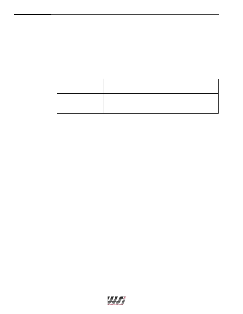
MCU
Port E (3:0)
Port E (7:4)
Port F (3:0)
Port F (7:4)
Port G (3:0)
Port G (7:4)
80C51XA
N/A
Addr (7:4)
N/A
Addr (7:4)
Addr (11:8)
Addr (15:12)
All Other
MCU with
Multiplexed
Bus
Addr (3:0)
Addr (7:4)
Addr (3:0)
Addr (7:4)
Addr (11:8)
Addr (15:12)
Table 21. I/OPort Latched Address Output Assignments
相關(guān)PDF資料 |
PDF描述 |
|---|---|
| PSD4235G2 | FLASH IN-SYSTEM PROGRAMMABLE (ISP) PERIPHERALS FOR 16-BIT MCUS (5V SUPPLY) |
| PSD4235G2V | -200V 100kRad Hi-Rel Single P-Channel TID Hardened MOSFET in a TO-254AA package; A JANSR2N7426 with Standard Packaging |
| PSD4235G1-B-12J | Flash In-System Programmable ISP Peripherals For 16-bit MCUs 5V Supply |
| PSD4235F2-A-12J | Flash In-System Programmable ISP Peripherals For 16-bit MCUs 5V Supply |
| PSD4235G2-A-12J | Flash In-System Programmable ISP Peripherals For 16-bit MCUs 5V Supply |
相關(guān)代理商/技術(shù)參數(shù) |
參數(shù)描述 |
|---|---|
| PSD4235G2-70U | 功能描述:SPLD - 簡(jiǎn)單可編程邏輯器件 5.0V 4M 70ns RoHS:否 制造商:Texas Instruments 邏輯系列:TICPAL22V10Z 大電池?cái)?shù)量:10 最大工作頻率:66 MHz 延遲時(shí)間:25 ns 工作電源電壓:4.75 V to 5.25 V 電源電流:100 uA 最大工作溫度:+ 75 C 最小工作溫度:0 C 安裝風(fēng)格:Through Hole 封裝 / 箱體:DIP-24 |
| PSD4235G2-90U | 功能描述:CPLD - 復(fù)雜可編程邏輯器件 5.0V 4M 90ns RoHS:否 制造商:Lattice 系列: 存儲(chǔ)類型:EEPROM 大電池?cái)?shù)量:128 最大工作頻率:333 MHz 延遲時(shí)間:2.7 ns 可編程輸入/輸出端數(shù)量:64 工作電源電壓:3.3 V 最大工作溫度:+ 90 C 最小工作溫度:0 C 封裝 / 箱體:TQFP-100 |
| PSD4235G2-90UI | 功能描述:CPLD - 復(fù)雜可編程邏輯器件 5.0V 4M 90ns RoHS:否 制造商:Lattice 系列: 存儲(chǔ)類型:EEPROM 大電池?cái)?shù)量:128 最大工作頻率:333 MHz 延遲時(shí)間:2.7 ns 可編程輸入/輸出端數(shù)量:64 工作電源電壓:3.3 V 最大工作溫度:+ 90 C 最小工作溫度:0 C 封裝 / 箱體:TQFP-100 |
| PSD4235G2V-12UI | 功能描述:CPLD - 復(fù)雜可編程邏輯器件 3.3V 4M 120ns RoHS:否 制造商:Lattice 系列: 存儲(chǔ)類型:EEPROM 大電池?cái)?shù)量:128 最大工作頻率:333 MHz 延遲時(shí)間:2.7 ns 可編程輸入/輸出端數(shù)量:64 工作電源電壓:3.3 V 最大工作溫度:+ 90 C 最小工作溫度:0 C 封裝 / 箱體:TQFP-100 |
| PSD4235G2V-90U | 功能描述:CPLD - 復(fù)雜可編程邏輯器件 3.3V 4M 90ns RoHS:否 制造商:Lattice 系列: 存儲(chǔ)類型:EEPROM 大電池?cái)?shù)量:128 最大工作頻率:333 MHz 延遲時(shí)間:2.7 ns 可編程輸入/輸出端數(shù)量:64 工作電源電壓:3.3 V 最大工作溫度:+ 90 C 最小工作溫度:0 C 封裝 / 箱體:TQFP-100 |
發(fā)布緊急采購(gòu),3分鐘左右您將得到回復(fù)。