- 您現(xiàn)在的位置:買賣IC網(wǎng) > PDF目錄299790 > PSD4235G2-A-15U (STMICROELECTRONICS) 4M X 1 FLASH, 52 I/O, PIA-GENERAL PURPOSE, PQFP80 PDF資料下載
參數(shù)資料
| 型號(hào): | PSD4235G2-A-15U |
| 廠商: | STMICROELECTRONICS |
| 元件分類: | 微控制器/微處理器 |
| 英文描述: | 4M X 1 FLASH, 52 I/O, PIA-GENERAL PURPOSE, PQFP80 |
| 封裝: | PLASTIC, TQFP-80 |
| 文件頁(yè)數(shù): | 11/104頁(yè) |
| 文件大小: | 1114K |
| 代理商: | PSD4235G2-A-15U |
第1頁(yè)第2頁(yè)第3頁(yè)第4頁(yè)第5頁(yè)第6頁(yè)第7頁(yè)第8頁(yè)第9頁(yè)第10頁(yè)當(dāng)前第11頁(yè)第12頁(yè)第13頁(yè)第14頁(yè)第15頁(yè)第16頁(yè)第17頁(yè)第18頁(yè)第19頁(yè)第20頁(yè)第21頁(yè)第22頁(yè)第23頁(yè)第24頁(yè)第25頁(yè)第26頁(yè)第27頁(yè)第28頁(yè)第29頁(yè)第30頁(yè)第31頁(yè)第32頁(yè)第33頁(yè)第34頁(yè)第35頁(yè)第36頁(yè)第37頁(yè)第38頁(yè)第39頁(yè)第40頁(yè)第41頁(yè)第42頁(yè)第43頁(yè)第44頁(yè)第45頁(yè)第46頁(yè)第47頁(yè)第48頁(yè)第49頁(yè)第50頁(yè)第51頁(yè)第52頁(yè)第53頁(yè)第54頁(yè)第55頁(yè)第56頁(yè)第57頁(yè)第58頁(yè)第59頁(yè)第60頁(yè)第61頁(yè)第62頁(yè)第63頁(yè)第64頁(yè)第65頁(yè)第66頁(yè)第67頁(yè)第68頁(yè)第69頁(yè)第70頁(yè)第71頁(yè)第72頁(yè)第73頁(yè)第74頁(yè)第75頁(yè)第76頁(yè)第77頁(yè)第78頁(yè)第79頁(yè)第80頁(yè)第81頁(yè)第82頁(yè)第83頁(yè)第84頁(yè)第85頁(yè)第86頁(yè)第87頁(yè)第88頁(yè)第89頁(yè)第90頁(yè)第91頁(yè)第92頁(yè)第93頁(yè)第94頁(yè)第95頁(yè)第96頁(yè)第97頁(yè)第98頁(yè)第99頁(yè)第100頁(yè)第101頁(yè)第102頁(yè)第103頁(yè)第104頁(yè)
Obsolete
Product(s)
- Obsolete
Product(s)
Pin description
PSD4135G2, PSD4135G2V
Doc ID 7838 Rev 2
2
Pin description
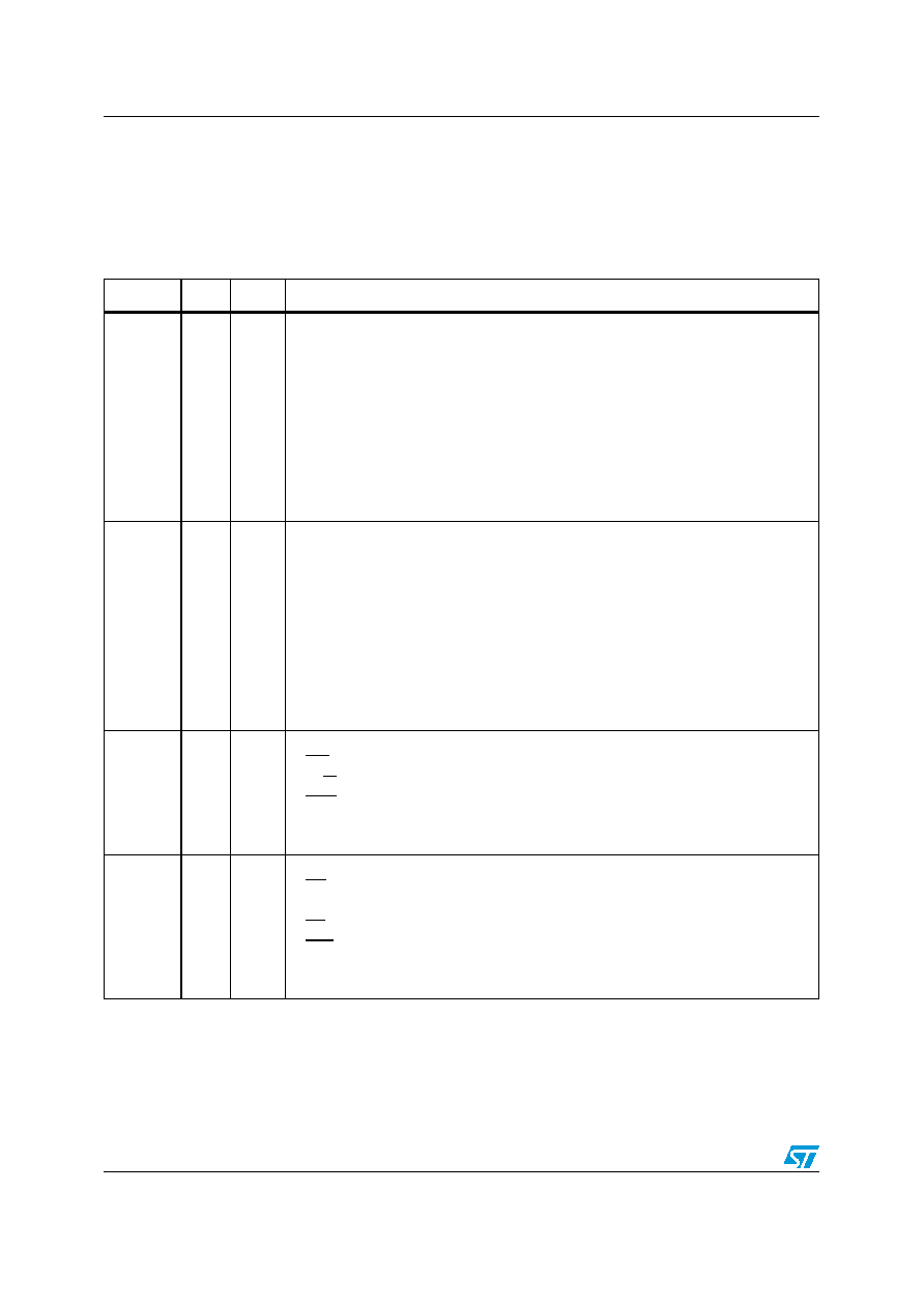
Table 2 describes the pin names and pin functions of the PSD4135G2 and PSD4135G2V.
Pins that have multiple names and/or functions are defined using PSDsoft Express.
Table 2.
Pin description
Pin name
Pin
Type
Description
ADIO0-
ADIO7
3-7
10-12
I/O
This is the lower Address/Data port. Connect your MCU address or address/data bus
according to the following rules:
1. If your MCU has a multiplexed address/data bus where the data is multiplexed with
the lower address bits, connect AD0-AD7 to this port.
2. If your MCU does not have a multiplexed address/data bus, connect A0-A7 to this
port.
3. If you are using an 80C51XA in burst mode, connect A4/D0 through A11/D7 to this
port.
ALE or AS latches the address. The PSD drives data out only if the READ signal is
active and one of the PSD functional blocks has been selected. The addresses on
this port are passed to the PLDs.
ADIO8-
ADIO15
13-20
I/O
This is the upper Address/Data port. Connect your MCU address or address/data bus
according to the following rules:
1. If your MCU has a multiplexed address/data bus where the data is multiplexed with
the upper address bits, connect A8-A15 to this port.
2. If your MCU does not have a multiplexed address/data bus, connect A8-A15 to this
port.
3. If you are using an 80C51XA in burst mode, connect A12/D8 through A19/D15 to
this port.
ALE or AS latches the address. The PSD drives data out only if the READ signal is
active and one of the PSD functional blocks has been selected. The addresses on
this port are passed to the PLDs.
CNTL0
59
I
The following control signals can be connected to this pin, based on your MCU:
1. WR - active low, Write Strobe input.
2. R_W - active high, READ/active low WRITE input.
3. WRL - active low, WRITE to low-byte.
This pin is connected to the PLDs. Therefore, these signals can be used in decode
and other logic equations.
CNTL1
60
I
The following control signals can be connected to this pin, based on your MCU:
1. RD - active low, Read Strobe input.
2. E - E clock input.
3. DS - active low, Data Strobe input.
4. LDS - active low, Strobe for low data byte.
This pin is connected to the PLDs. Therefore, these signals can be used in decode
and other logic equations.
相關(guān)PDF資料 |
PDF描述 |
|---|---|
| PSD4235G2-A-20UI | 4M X 1 FLASH, 52 I/O, PIA-GENERAL PURPOSE, PQFP80 |
| PSD813F2A-15JI | 128K X 8 FLASH, 27 I/O, PIA-GENERAL PURPOSE, PQCC52 |
| PSD834F2VA-15MI | 256K X 8 FLASH, 27 I/O, PIA-GENERAL PURPOSE, PQFP52 |
| PSD854F2A-90MT | 256K X 8 FLASH, 27 I/O, PIA-GENERAL PURPOSE, PQFP52 |
| PSD854F2A-90UT | 256K X 8 FLASH, 27 I/O, PIA-GENERAL PURPOSE, PQFP64 |
相關(guān)代理商/技術(shù)參數(shù) |
參數(shù)描述 |
|---|---|
| PSD4235G2V-12UI | 功能描述:CPLD - 復(fù)雜可編程邏輯器件 3.3V 4M 120ns RoHS:否 制造商:Lattice 系列: 存儲(chǔ)類型:EEPROM 大電池?cái)?shù)量:128 最大工作頻率:333 MHz 延遲時(shí)間:2.7 ns 可編程輸入/輸出端數(shù)量:64 工作電源電壓:3.3 V 最大工作溫度:+ 90 C 最小工作溫度:0 C 封裝 / 箱體:TQFP-100 |
| PSD4235G2V-90U | 功能描述:CPLD - 復(fù)雜可編程邏輯器件 3.3V 4M 90ns RoHS:否 制造商:Lattice 系列: 存儲(chǔ)類型:EEPROM 大電池?cái)?shù)量:128 最大工作頻率:333 MHz 延遲時(shí)間:2.7 ns 可編程輸入/輸出端數(shù)量:64 工作電源電壓:3.3 V 最大工作溫度:+ 90 C 最小工作溫度:0 C 封裝 / 箱體:TQFP-100 |
| PSD4256G6V-10UI | 功能描述:CPLD - 復(fù)雜可編程邏輯器件 3.3V 8M 100ns RoHS:否 制造商:Lattice 系列: 存儲(chǔ)類型:EEPROM 大電池?cái)?shù)量:128 最大工作頻率:333 MHz 延遲時(shí)間:2.7 ns 可編程輸入/輸出端數(shù)量:64 工作電源電壓:3.3 V 最大工作溫度:+ 90 C 最小工作溫度:0 C 封裝 / 箱體:TQFP-100 |
| PSD4-36 | 制造商:Tamura Corporation of America 功能描述: |
| PSD-45 | 制造商:MEANWELL 制造商全稱:Mean Well Enterprises Co., Ltd. 功能描述:45W DC-DC Single Output Switching Power Supply |
發(fā)布緊急采購(gòu),3分鐘左右您將得到回復(fù)。