- 您現(xiàn)在的位置:買賣IC網(wǎng) > PDF目錄367799 > PC745BVZFU400LD MICROPROCESSOR|32-BIT|CMOS|BGA|255PIN|PLASTIC PDF資料下載
參數(shù)資料
| 型號: | PC745BVZFU400LD |
| 英文描述: | MICROPROCESSOR|32-BIT|CMOS|BGA|255PIN|PLASTIC |
| 中文描述: | 微處理器| 32位|的CMOS | BGA封裝| 255PIN |塑料 |
| 文件頁數(shù): | 36/48頁 |
| 文件大小: | 276K |
| 代理商: | PC745BVZFU400LD |
第1頁第2頁第3頁第4頁第5頁第6頁第7頁第8頁第9頁第10頁第11頁第12頁第13頁第14頁第15頁第16頁第17頁第18頁第19頁第20頁第21頁第22頁第23頁第24頁第25頁第26頁第27頁第28頁第29頁第30頁第31頁第32頁第33頁第34頁第35頁當前第36頁第37頁第38頁第39頁第40頁第41頁第42頁第43頁第44頁第45頁第46頁第47頁第48頁
36/48
PC755B/745B
The COP header shown in Figure 24 adds many benefits—breakpoints, watchpoints, register and memory examination/modification
and other standard debugger features are possible through this interface – and can be as inexpensive as an unpopulated footprint for
a header to be added when needed.
System design information
The COP interface has a standard header for connection to the target system, based on the 0.025” square-post 0.100” centered
header assembly (often called a “Berg” header). The connector typically has pin 14 removed as a connector key.
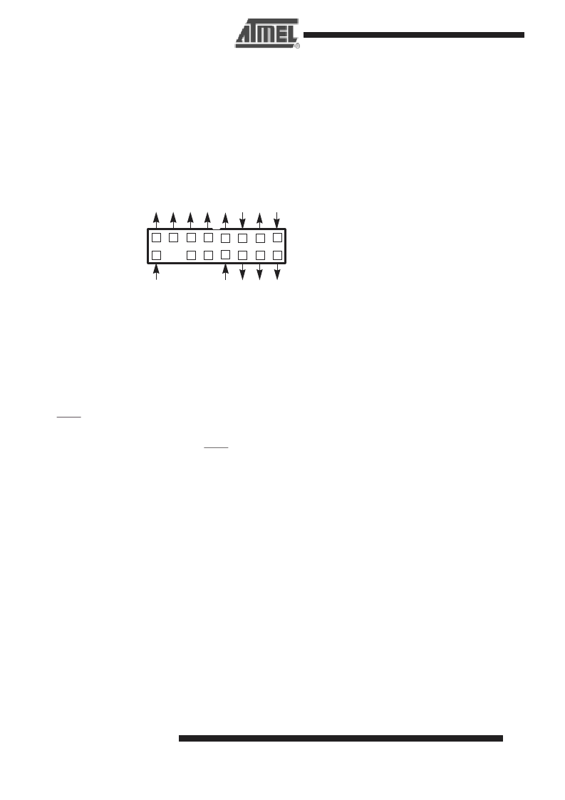
Figure 24 shows the COP connector diagram.
3
C
13
9
5
1
6
10
2
TOP VIEW
15
11
7
16
12
8
4
KEY
H
S
T
R
T
T
T
G
T
V
Pins 10, 12 and 14 are no–connects.
Pin 14 is not physically present
Q
C
Figure 24 : COP Connector Diagram
There is no standardized way to number the COP header shown in Figure 24; consequently, many different pin numbers have been
observed from emulator vendors. Some are numbered top-to-bottom then left-to-right, while others use left-to-right then top-to-bot-
tom, while still others number the pins counter clockwise from pin one (as with an IC). Regardless of the numbering, the signal place-
ment recommended in Figure 24 is common to all known emulators.
The QACK signal shown in Table 15 is usually hooked up to the PCI bridge chip in a system and is an input to the PC755B informing it
that it can go into the quiescent state. Under normal operation this occurs during a low power mode selection. In order for
COP to work
the PC755B must see this signal asserted (pulled down). While shown on the COP header, not all emulator products drive this signal.
To preserve correct power down operation, QACK should be merged so that it also can be driven by the PCI bridge.
相關(guān)PDF資料 |
PDF描述 |
|---|---|
| PC755BMZFU300LD | MICROPROCESSOR|32-BIT|CMOS|BGA|360PIN|PLASTIC |
| PC755BMZFU350LD | MICROPROCESSOR|32-BIT|CMOS|BGA|360PIN|PLASTIC |
| PC755BMZFU400LD | MICROPROCESSOR|32-BIT|CMOS|BGA|360PIN|PLASTIC |
| PC755BVZFU300LD | MICROPROCESSOR|32-BIT|CMOS|BGA|360PIN|PLASTIC |
| PC755 | PowerPC 755/745 RISC Microprocessor |
相關(guān)代理商/技術(shù)參數(shù) |
參數(shù)描述 |
|---|---|
| PC74631-1 | 制造商: 功能描述: 制造商:undefined 功能描述: |
| PC74HC00D | 制造商:未知廠家 制造商全稱:未知廠家 功能描述:Quad 2-input NAND Gate |
| PC74HC04T | 制造商:NXP Semiconductors 功能描述: |
| PC74HC08N | 制造商:NXP Semiconductors 功能描述:74HC08N |
| PC74HC244T | 制造商:NXP Semiconductors 功能描述: |
發(fā)布緊急采購,3分鐘左右您將得到回復(fù)。