- 您現(xiàn)在的位置:買賣IC網(wǎng) > PDF目錄361089 > NCN6000 (ON SEMICONDUCTOR) Compact Smart Card Interface IC(智能卡接口集成電路) PDF資料下載
參數(shù)資料
| 型號(hào): | NCN6000 |
| 廠商: | ON SEMICONDUCTOR |
| 英文描述: | Compact Smart Card Interface IC(智能卡接口集成電路) |
| 中文描述: | 緊湊型智能卡接口IC(智能卡接口集成電路) |
| 文件頁數(shù): | 7/36頁 |
| 文件大小: | 358K |
| 代理商: | NCN6000 |
第1頁第2頁第3頁第4頁第5頁第6頁當(dāng)前第7頁第8頁第9頁第10頁第11頁第12頁第13頁第14頁第15頁第16頁第17頁第18頁第19頁第20頁第21頁第22頁第23頁第24頁第25頁第26頁第27頁第28頁第29頁第30頁第31頁第32頁第33頁第34頁第35頁第36頁
NCN6000
http://onsemi.com
7
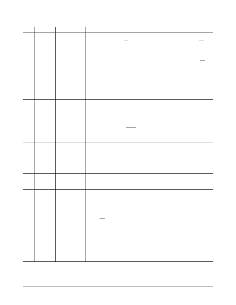
PIN FUNCTIONS AND DESCRIPTION (continued)
Pin
Name
Description
Type
8
I/O
Input/Output
Pull Up
This pin is connected to an external microcontroller interface. A bidirectional level translator
adapts the serial I/O signal between the smart card and the microcontroller. The level
translator is enabled when CS = L. The signal present on this pin is latched when CS = H.
This pin is also used in programming mode (Tables 1, 2 and 3, Figures 4 and 5).
9
INT
OUTPUT
Pull Down
This pin is activated LOW when a card has been inserted and detected by the interface or
when the NCN6000 reports Vbat or CRD_VCC status (See Table 6). The signal is reset to
a logic 1 on the rising edge of either CS or PWR_ON. The Collector open mode makes
possible the wired AND/OR external logic. When two or more interfaces share the INT
function with a single microcontroller, the software must poll the STATUS pin to identify the
origin of the interrupt (Figure 5).
10
CLOCK_IN
CLOCK INPUT
High Impedance
This pin can be connected to either the microcontroller master clock, or to any clock signal,
to drive the external smart cards. The signal is fed to internal clock selector circuit and
translated to the CRD_CLK pin at either the same frequency, or divided by 2 or 4 or 8,
depending upon the programming mode (Tables 1, 2 and 3).
Care must be observed, at PCB level, to minimize the pickup noise coming from the
CLOCK_IN line. It is recommended to put a shield, built with a 10 mil copper track, around
this line and terminated to the GND.
11
CRD_DET
INPUT
The signal coming from the external card connector is used to detect the presence of the
card. A builtin pull up low current source makes this pin active LOW or HIGH, assuming
one side of the external switch is connected to ground. At Vbat start up, the default
condition is Normally Open switch, negative going insertion detection. The Normally
Closed switch, positive going insertion detection, can be defined by programming the
NCN6000 accordingly. In this case, the polarity must be set up during the first cycles of the
system initialization, otherwise an already inserted card will not be detected by the chip.
12
CRD_RST
OUTPUT
This pin is connected to the RESET pin of the card connector. A level translator adapts the
RESET signal from the microcontroller to the external card. The output current is internally
limited to 15 mA. The CRD_RST is validated when PWR_ON = H and PGM = H and hard
wired to Ground when the card is deactivated.
13
CRD_CLK
OUTPUT
This pin is connected to the CLK pin of the card connector. The CRD_CLK signal comes
from the clock selector circuit output. Combining A0, A1, PGM and I/O, as depicted in
Table 3 and Figure 3, programs the clock selection. This signal can be forced into a
standby mode with CRD_CLK either High or Low, depending upon the mode defined by
the programming sequence (Tables 1, 2 and 3 and Figure 4).
Care must be observed, at PCB level, to minimize the pickup noise coming from the
CRD_CLK line. It is recommended to put a shield, built with a 10mil copper track, around
this line and terminated to the GND.
14
CRD_IO
I/O
This pin handles the connection to the serial I/O pin of the card connector. A bidirectional
level translator adapts the serial I/O signal between the card and the microcontroller. The
CRD_IO pin current is internally limited to 15 mA. A builtin register holds the previous
state presents on the I/O input pin.
15
CRD_VCC
POWER
This pin provides the power to the external card. It is the logic level “1” for CRD_IO,
CRD_RST and CRD_CLK signals. The energy stored by the DCDC external inductor
Lout must be smoothed by a 10 F capacitor, associated with a 100 nF ceramic in parallel,
connected across CRD_VCC and GND. In the event of a CRD_VCC U
VLOW
voltage, the
NCN6000 detects the situation and feedback the information in the STATUS bit. The device
does not take any further action, particularly the DCDC converter is neither stopped nor
reprogrammed by the NCN6000. It is up to the external MPU to handle the situation.
However, when the CRD_VCC is overloaded, the NCN6000 shut off the DCDC converter,
pulls the INT pin Low and reports the fault in the STATUS register.
16
GROUND
SIGNAL
The logic and low level analog signals shall be connected to this ground pin. This pin must
be externally connected to the PWR_GND pin 17. The designer must make sure no high
current transients are shared with the low signal currents flowing into this pin.
17
PWR_GND
POWER
This pin is the Power Ground associated with the builtin DCDC converter and must be
connected to the system ground together with GROUND pin 11. Using good quality ground
plane is recommended to avoid spikes on the logic signal lines.
18
Lout_L
POWER
The High Side of the external inductor is connected between this pin and Lout_H to provide
the DCDC function. The builtin MOS devices provide the switching function together with
the CRD_VCC voltage rectification.
相關(guān)PDF資料 |
PDF描述 |
|---|---|
| NCN6001DTBR2 | Compact Smart Card Interface IC |
| NCN6001 | Compact Smart Card Interface IC |
| NCN6004AFTBR2 | Dual SAM/SIM Interface Integrated Circuit |
| NCN6004A | Dual SAM/SIM Interface Integrated Circuit |
| NCN6010DTBR2 | SIM Card Supply and Level Shifter |
相關(guān)代理商/技術(shù)參數(shù) |
參數(shù)描述 |
|---|---|
| NCN6000/D | 制造商:未知廠家 制造商全稱:未知廠家 功能描述:Compact Smart Card Interface IC |
| NCN6000DTB | 功能描述:輸入/輸出控制器接口集成電路 2.7V POS/ATM Smart RoHS:否 制造商:Silicon Labs 產(chǎn)品: 輸入/輸出端數(shù)量: 工作電源電壓: 最大工作溫度:+ 85 C 最小工作溫度:- 40 C 安裝風(fēng)格:SMD/SMT 封裝 / 箱體:QFN-64 封裝:Tray |
| NCN6000DTBG | 功能描述:輸入/輸出控制器接口集成電路 2.7V POS/ATM Smart Card Interface RoHS:否 制造商:Silicon Labs 產(chǎn)品: 輸入/輸出端數(shù)量: 工作電源電壓: 最大工作溫度:+ 85 C 最小工作溫度:- 40 C 安裝風(fēng)格:SMD/SMT 封裝 / 箱體:QFN-64 封裝:Tray |
| NCN6000DTBR2 | 功能描述:輸入/輸出控制器接口集成電路 2.7V POS/ATM Smart RoHS:否 制造商:Silicon Labs 產(chǎn)品: 輸入/輸出端數(shù)量: 工作電源電壓: 最大工作溫度:+ 85 C 最小工作溫度:- 40 C 安裝風(fēng)格:SMD/SMT 封裝 / 箱體:QFN-64 封裝:Tray |
| NCN6000DTBR2G | 功能描述:輸入/輸出控制器接口集成電路 2.7V POS/ATM Smart Card Interface RoHS:否 制造商:Silicon Labs 產(chǎn)品: 輸入/輸出端數(shù)量: 工作電源電壓: 最大工作溫度:+ 85 C 最小工作溫度:- 40 C 安裝風(fēng)格:SMD/SMT 封裝 / 箱體:QFN-64 封裝:Tray |
發(fā)布緊急采購,3分鐘左右您將得到回復(fù)。