- 您現(xiàn)在的位置:買賣IC網(wǎng) > PDF目錄224506 > MT55L256L32FT-12 256K X 32 ZBT SRAM, 9 ns, PQFP100 PDF資料下載
參數(shù)資料
| 型號(hào): | MT55L256L32FT-12 |
| 元件分類: | SRAM |
| 英文描述: | 256K X 32 ZBT SRAM, 9 ns, PQFP100 |
| 封裝: | PLASTIC, TQFP-100 |
| 文件頁數(shù): | 9/25頁 |
| 文件大小: | 300K |
| 代理商: | MT55L256L32FT-12 |
17
8Mb: 512K x 18, 256K x 32/36 Flow-Through ZBT SRAM
Micron Technology, Inc., reserves the right to change products or specifications without notice.
MT55L512L18F_C.p65 – Rev. 2/02
2002, Micron Technology, Inc.
8Mb: 512K x 18, 256K x 32/36
FLOW-THROUGH ZBT SRAM
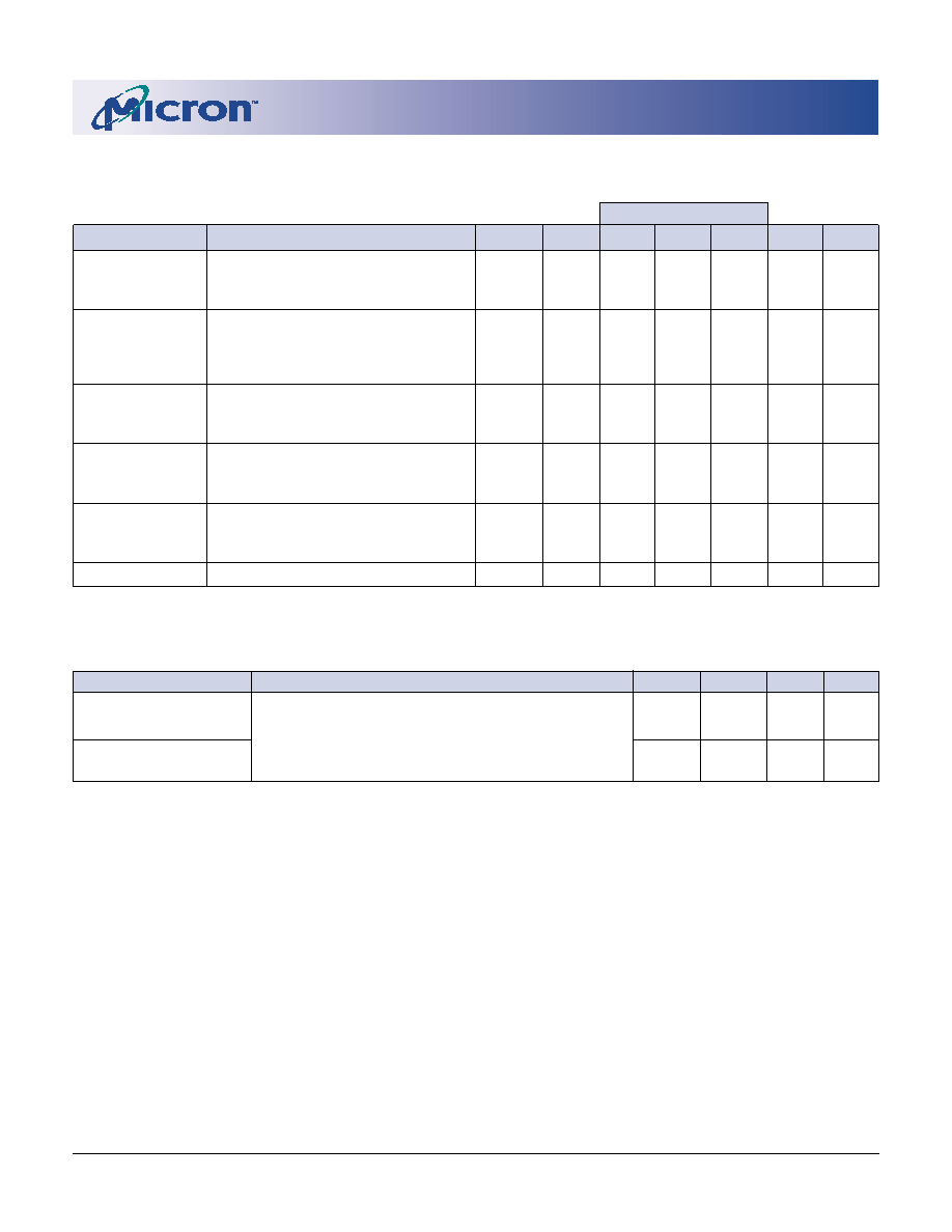
IDD OPERATING CONDITIONS AND MAXIMUM LIMITS
(Note 1) (0° C
≤ T
A ≤ +70° C; VDD = +3.3V ±0.165V unless otherwise noted)
DESCRIPTION
CONDITIONS
SYMBOL
TYP
-10
-11
-12
UNITS NOTES
Power Supply
Device selected; All inputs
≤ VIL
Current:Operating
or
≥ VIH; Cycle time ≥ tKC (MIN);
IDD
165
300
275
250
mA
2, 3, 4
VDD = MAX; Outputs open
Power Supply
Device selected; VDD = MAX;
Current: Idle
CKE#
≥ VIH;IDD1
10
28
22
20
mA
2, 3, 4
All inputs
≤ VSS + 0.2 or ≥ VDD - 0.2;
Cycle time
≥ tKC (MIN)
CMOS Standby
Device deselected; VDD = MAX;
All inputs
≤ VSS + 0.2 or ≥ VDD - 0.2;
ISB2
0.5
10
mA
3, 4
All inputs static; CLK frequency = 0
TTL Standby
Device deselected; VDD = MAX;
All inputs
≤ VIL or ≥ VIH;ISB3
6
252525
mA
3, 4
All inputs static; CLK frequency = 0
Clock Running
Device deselected; VDD = MAX;
ADV/LD#
≥ VIH; All inputs ≤ VSS + 0.2
ISB4
37
65
60
mA
3, 4
or
≥ VDD - 0.2; Cycle time ≥ tKC (MIN)
SnoozeMode
ZZ
≥ VIH
ISB2Z
0.5
10
mA
4
MAX
NOTE: 1. VDDQ = +3.3V ±0.165V for 3.3V I/O configuration; VDDQ = +2.5V +0.4V/-0.125V for 2.5V I/O configuration.
2. IDD is specified with no output current and increases with faster cycle times. IDDQ increases with faster cycle times and
greater output loading.
3. “ Device deselected” means device is in a deselected cycle as defined in the truth table. “ Device selected” means device
is active (not in deselected mode).
4. Typical values are measured at +3.3V, +25° C and 12ns cycle time.
5. This parameter is sampled.
TQFP THERMAL RESISTANCE
DESCRIPTION
CONDITIONS
SYMBOL
TYP
UNITS NOTES
Thermal Resistance
Test conditions follow standard test methods
θ
JA
40
° C/W
5
(Junction to Ambient)
and procedures for measuring thermal
Thermal Resistance
impedance, per EIA/JESD51.
θ
JC
8
° C/W
5
(Junction to Top of Case)
相關(guān)PDF資料 |
PDF描述 |
|---|---|
| MT55L512V18PF-6 | 512K X 18 ZBT SRAM, 3.5 ns, PBGA165 |
| MT57W4MH9CF-6 | 4M X 9 DDR SRAM, 0.5 ns, PBGA165 |
| MT58L128L36D1T-5IT | 128K X 36 STANDARD SRAM, 2.8 ns, PQFP100 |
| MT58L128V36P1B-4 | 128K X 36 STANDARD SRAM, 2.3 ns, PBGA119 |
| MT58L32L36PT-7.5 | 32K X 36 CACHE SRAM, 4.2 ns, PQFP100 |
相關(guān)代理商/技術(shù)參數(shù) |
參數(shù)描述 |
|---|---|
| MT55L256L32FT-12IT | 制造商:Rochester Electronics LLC 功能描述:- Bulk |
| MT55L256L32P | 制造商:MICRON 制造商全稱:Micron Technology 功能描述:8Mb ZBT SRAM |
| MT55L256L32PF-10 | 制造商:Micron Technology Inc 功能描述: |
| MT55L256L32PT10 | 制造商:MICRON 功能描述:* |
| MT55L256L32PT-10 | 制造商:Cypress Semiconductor 功能描述:SRAM Chip Sync Quad 3.3V 8M-Bit 256K x 32 5ns 100-Pin TQFP 制造商:Micron Technology Inc 功能描述: |
發(fā)布緊急采購(gòu),3分鐘左右您將得到回復(fù)。