- 您現(xiàn)在的位置:買賣IC網(wǎng) > PDF目錄45276 > MQ80C52TXXX-20:D (ATMEL CORP) 8-BIT, MROM, 20 MHz, MICROCONTROLLER, CQFP44 PDF資料下載
參數(shù)資料
| 型號: | MQ80C52TXXX-20:D |
| 廠商: | ATMEL CORP |
| 元件分類: | 微控制器/微處理器 |
| 英文描述: | 8-BIT, MROM, 20 MHz, MICROCONTROLLER, CQFP44 |
| 封裝: | CERAMIC, QFP-44 |
| 文件頁數(shù): | 39/81頁 |
| 文件大?。?/td> | 663K |
第1頁第2頁第3頁第4頁第5頁第6頁第7頁第8頁第9頁第10頁第11頁第12頁第13頁第14頁第15頁第16頁第17頁第18頁第19頁第20頁第21頁第22頁第23頁第24頁第25頁第26頁第27頁第28頁第29頁第30頁第31頁第32頁第33頁第34頁第35頁第36頁第37頁第38頁當(dāng)前第39頁第40頁第41頁第42頁第43頁第44頁第45頁第46頁第47頁第48頁第49頁第50頁第51頁第52頁第53頁第54頁第55頁第56頁第57頁第58頁第59頁第60頁第61頁第62頁第63頁第64頁第65頁第66頁第67頁第68頁第69頁第70頁第71頁第72頁第73頁第74頁第75頁第76頁第77頁第78頁第79頁第80頁第81頁
44
ATtiny28L/V
1062F–AVR–07/06
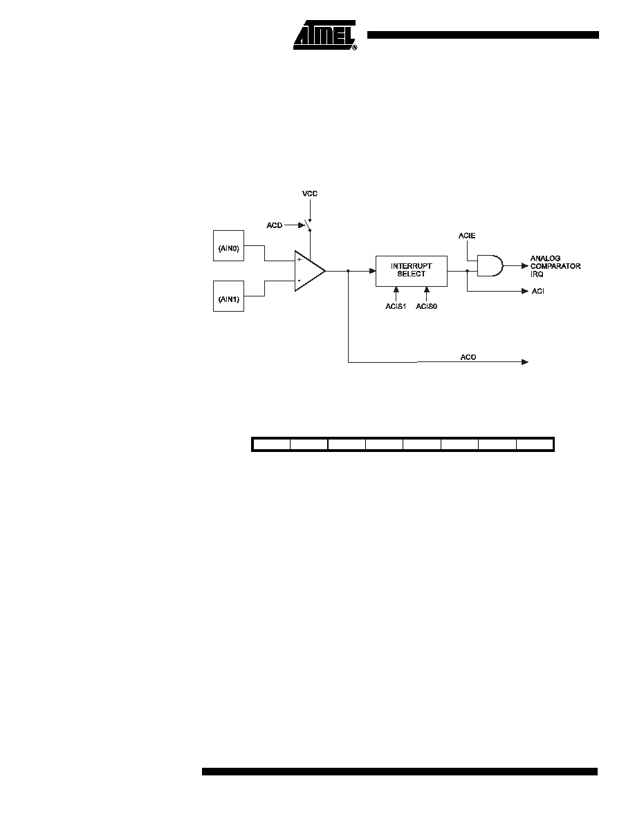
Analog Comparator
The analog comparator compares the input values on the positive input PB0 (AIN0) and
negative input PB1 (AIN1). When the voltage on the positive input PB0 (AIN0) is higher
than the voltage on the negative input PB1 (AIN1), the Analog Comparator Output
(ACO) is set (one). The comparator can trigger a separate interrupt exclusive to the ana-
log comparator. The user can select interrupt triggering on comparator output rise, fall or
toggle. A block diagram of the comparator and its surrounding logic is shown in Figure
36.
Figure 36. Analog Comparator Block Diagram
Register Description
Analog Comparator Control
and Status Register – ACSR
Bit 7 – ACD: Analog Comparator Disable
When this bit is set (one), the power to the analog comparator is switched off. This bit
can be set at any time to turn off the analog comparator. When changing the ACD bit,
the Analog Comparator Interrupt must be disabled by clearing the ACIE bit in ACSR.
Otherwise, an interrupt can occur when the bit is changed. To use the analog compara-
tor, the user must clear this bit.
Bit 6 – Res: Reserved Bit
This bit is a reserved bit in the ATtiny28 and will always read as zero.
Bit 5 – ACO: Analog Comparator Output
ACO is directly connected to the comparator output.
Bit 4 – ACI: Analog Comparator Interrupt Flag
This bit is set (one) when a comparator output event triggers the interrupt mode defined
by ACI1 and ACI0. The Analog Comparator Interrupt routine is executed if the ACIE bit
is set (one) and the I-bit in SREG is set (one). ACI is cleared by hardware when execut-
PB0
PB1
Bit
7654
321
0
$08
ACD
–
ACO
ACI
ACIE
–
ACIS1
ACIS0
ACSR
Read/Write
R/W
R
R/W
R
R/W
Initial Value
1
0
X
0
相關(guān)PDF資料 |
PDF描述 |
|---|---|
| MR80C32-20/883:RD | 8-BIT, 20 MHz, MICROCONTROLLER, CQCC44 |
| MR80C32-16/883R | 8-BIT, 16 MHz, MICROCONTROLLER, CQCC44 |
| MC80C52CXXX-30P883 | 8-BIT, MROM, 30 MHz, MICROCONTROLLER, CDIP40 |
| MR80C32-20/883:RD | 8-BIT, 20 MHz, MICROCONTROLLER, CQCC44 |
| MC80C52XXX-16SBD | 8-BIT, MROM, 16 MHz, MICROCONTROLLER, CDIP40 |
相關(guān)代理商/技術(shù)參數(shù) |
參數(shù)描述 |
|---|---|
| MQ82370-20 | 制造商:Rochester Electronics LLC 功能描述:- Bulk |
| MQ8238020 | 制造商:Intel 功能描述:CONTROLLER: OTHER |
| MQ82380-20 | 制造商:Rochester Electronics LLC 功能描述:- Bulk |
| MQ82380-20/R | 制造商:Rochester Electronics LLC 功能描述: |
| MQ82592 | 制造商:Rochester Electronics LLC 功能描述:- Bulk |
發(fā)布緊急采購,3分鐘左右您將得到回復(fù)。