- 您現(xiàn)在的位置:買賣IC網(wǎng) > PDF目錄69037 > MPC92432AE (INTEGRATED DEVICE TECHNOLOGY INC) 1360 MHz, OTHER CLOCK GENERATOR, PQFP48 PDF資料下載
參數(shù)資料
| 型號(hào): | MPC92432AE |
| 廠商: | INTEGRATED DEVICE TECHNOLOGY INC |
| 元件分類: | 時(shí)鐘產(chǎn)生/分配 |
| 英文描述: | 1360 MHz, OTHER CLOCK GENERATOR, PQFP48 |
| 封裝: | ROHS COMPLIANT, LQFP-48 |
| 文件頁(yè)數(shù): | 3/19頁(yè) |
| 文件大?。?/td> | 611K |
| 代理商: | MPC92432AE |
第1頁(yè)第2頁(yè)當(dāng)前第3頁(yè)第4頁(yè)第5頁(yè)第6頁(yè)第7頁(yè)第8頁(yè)第9頁(yè)第10頁(yè)第11頁(yè)第12頁(yè)第13頁(yè)第14頁(yè)第15頁(yè)第16頁(yè)第17頁(yè)第18頁(yè)第19頁(yè)
Advanced Clock Drivers Devices
Freescale Semiconductor
11
MPC92432
Programming the I2C Interface
The 7-bit I2C slave address of the MPC92432 synthesizer
is a combination of a 5-bit fixed addresses and two variable
bits which are set by the hardware pins ADR[1:0]. Bit 0 of the
MPC92432 slave address is used by the bus controller to
select either the read or write mode. ’0’ indicates a
transmission (I2C-WRITE) to the MPC92432. ’1’ indicates a
request for data (I2C-READ) from the synthesizer. The
hardware pins ADR1 and ADR0 and should be individually
set by the user to avoid address conflicts of multiple
MPC92432 devices on the same I2C bus.
Write Mode (R/W = 0)
The configuration registers are written by the bus
controller by the initiation of a write transfer with the
MPC92432 slave address (first byte), followed by the address
of the configuration register (second byte: 0x00, 0x01 or
0xF0), and the configuration data byte (third byte). This
transfer may be followed by writing more registers by sending
the configuration register address followed by one data byte.
Each byte sent by the bus controller is acknowledged by the
MPC92432. The transfer ends by a stop bit sent by the bus
controller. The number of configuration data bytes and the
write sequence are not restricted.
Read Mode (R/W = 1)
The configuration registers are read by the bus controller
by the initiation of a read transfer. The MPC92432 supports
read transfers immediately after the first byte without a
change in the transfer direction. Immediately after the bus
controller sends the slave address, the MPC92432
acknowledges and then sends both configuration register
PLL_L and PLL_H (back-to-back) to the bus controller. The
CMD register cannot be read. In order to read the two
synthesizer registers and the current PLL configuration
setting, the user can 1) read PLL_L, PLL_H, write the GET
command (loads the current configuration into PLL_L,
PLL_H) and read PLL_L, PLL_H again. Note that the PLL_L,
PLL_H registers and divider settings may not be equivalent
after the following cases:
a.
Writing the INC command
b.
Writing the DEC command
c.
Writing PLL_L, PLL_H registers with a new
configuration and not writing the LOAD command.
Device Startup
General Device Configuration
It is recommended to reset the MPC92432 during or
immediately after the system powers up (MR = 0). The device
acquires an initial PLL divider configuration through the
parallel interface pins M[9:0], NA[2:0], N, and P(1) with the
low-to-high transition of MR(2). PLL frequency lock is
achieved within the specified lock time (tLOCK) and is
indicated by an assertion of the LOCK signal which
completes the startup procedure. It is recommended to
disable the outputs (CLK_STOPx = 0) until PLL lock is
achieved to suppress output frequency transitions. The
output frequency can be reconfigured at any time through
either the parallel or the serial interface.
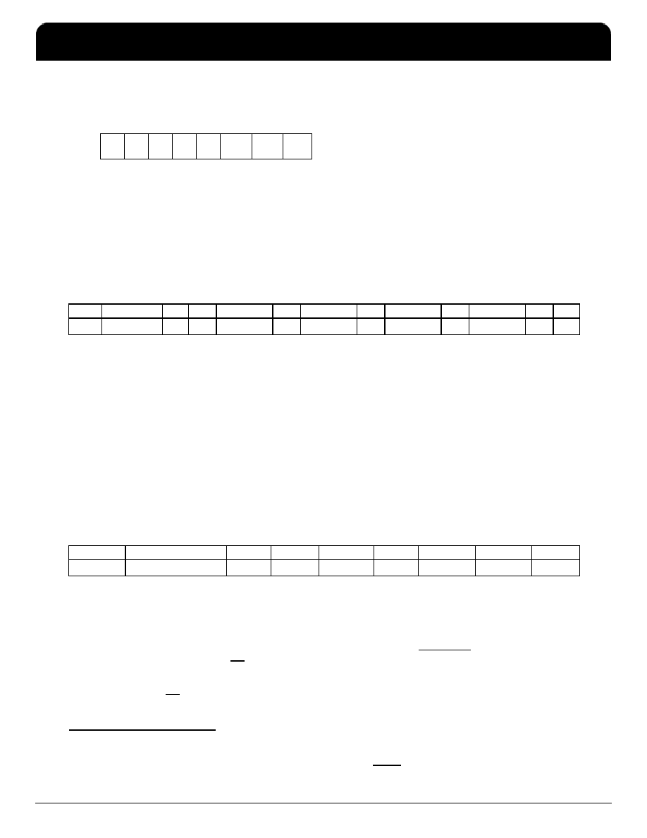
Table 18. I2C Slave Address
Bit
76543
2
1
0
Value
10110Pin
ADR1
Pin
ADR0
R/W
Table 19. Complete Configuration Register Write Transfer
1 bit
7 bits
1 bit
8 bits
1 bit
8 bits
1 bit
8 bits
1 bit
8 bits
1 bit
Start
Slave address
R/W
ACK
&PLL_H
ACK
Config-Byte 1
ACK
&PLL_L
ACK
Config-Byte 2
ACK
Stop
10110xx(1)
1. xx = state of ADR1, ADR0 pins
0
0x01Data0x00Data
Master
Mast Slave
Master
Slave
Master
Slave
Master
Slave
Master
Slave Mast
Table 20. Configuration Register Read Transfer
1 bit
7 bits
1 bit
8 bits
1 bit
8 bits
1 bit
Start
Slave address
R/W
ACK
PLL_L
ACK
PLL_H
ACK
Stop
10110xx(1)
1. xx = state of ADR1, ADR0 pins
1
Data
Master
Mast
Slave
Mast
Slave
Master
Slave
1. The parallel interface pins M[9:0], NA[2:0], N, and P may be left open (floating). In this case the initial PLL configuration will have the default
setting of M = 500, P = 1, NA[2:0] = 010, NB = 0, resulting in an internal VCO frequency of 2000 MHz (fref = 16 MHz) and an output frequency
of 250 MHz.
2. The initial PLL configuration is independent on the selected programming mode (PLOAD low or high)
MPC92432
1360 MHz Dual Output LVPECL Clock Synthesizer
NETCOM
IDT 1360 MHz Dual Output LVPECL Clock Synthesizer
Freescale Timing Solutions Organization has been acquired by Integrated Device Technology, Inc
MPC92432
11
相關(guān)PDF資料 |
PDF描述 |
|---|---|
| MPC9299FA | 400 MHz, OTHER CLOCK GENERATOR, PQFP32 |
| MPC930FA | 140 MHz, PROC SPECIFIC CLOCK GENERATOR, PQFP32 |
| MPC930FA | 140 MHz, PROC SPECIFIC CLOCK GENERATOR, PQFP32 |
| MPC972FA | 125 MHz, PROC SPECIFIC CLOCK GENERATOR, PQFP52 |
| MPC9850VF | 500 MHz, PROC SPECIFIC CLOCK GENERATOR, PBGA100 |
相關(guān)代理商/技術(shù)參數(shù) |
參數(shù)描述 |
|---|---|
| MPC92432AER2 | 功能描述:時(shí)鐘合成器/抖動(dòng)清除器 FSL 1360MHz Dual Out put LVPECL Clock Syn RoHS:否 制造商:Skyworks Solutions, Inc. 輸出端數(shù)量: 輸出電平: 最大輸出頻率: 輸入電平: 最大輸入頻率:6.1 GHz 電源電壓-最大:3.3 V 電源電壓-最小:2.7 V 封裝 / 箱體:TSSOP-28 封裝:Reel |
| MPC92432FA | 制造商:MOTOROLA 制造商全稱:Motorola, Inc 功能描述:1360 MHz Dual Output LVPECL Clock Synthesizer |
| MPC92433 | 制造商:FREESCALE 制造商全稱:Freescale Semiconductor, Inc 功能描述:1428 MHz Dual Output LVPECL Clock Synthesizer |
| MPC92433AE | 功能描述:時(shí)鐘合成器/抖動(dòng)清除器 FSL 1428MHz Dual Out put LVPECL Clock Syn RoHS:否 制造商:Skyworks Solutions, Inc. 輸出端數(shù)量: 輸出電平: 最大輸出頻率: 輸入電平: 最大輸入頻率:6.1 GHz 電源電壓-最大:3.3 V 電源電壓-最小:2.7 V 封裝 / 箱體:TSSOP-28 封裝:Reel |
| MPC92433AER2 | 功能描述:時(shí)鐘合成器/抖動(dòng)清除器 FSL 1428MHz Dual Out put LVPECL Clock Syn RoHS:否 制造商:Skyworks Solutions, Inc. 輸出端數(shù)量: 輸出電平: 最大輸出頻率: 輸入電平: 最大輸入頻率:6.1 GHz 電源電壓-最大:3.3 V 電源電壓-最小:2.7 V 封裝 / 箱體:TSSOP-28 封裝:Reel |
發(fā)布緊急采購(gòu),3分鐘左右您將得到回復(fù)。