- 您現(xiàn)在的位置:買賣IC網(wǎng) > PDF目錄45359 > MPC8309CVMAHFCA (FREESCALE SEMICONDUCTOR INC) 32-BIT, 417 MHz, RISC PROCESSOR, PBGA489 PDF資料下載
參數(shù)資料
| 型號(hào): | MPC8309CVMAHFCA |
| 廠商: | FREESCALE SEMICONDUCTOR INC |
| 元件分類: | 微控制器/微處理器 |
| 英文描述: | 32-BIT, 417 MHz, RISC PROCESSOR, PBGA489 |
| 封裝: | 19 X 19 MM, 1.61 MM HEIGHT, 0.80 MM PITCH, LEAD FREE, PLASTIC, MAPBGA-489 |
| 文件頁(yè)數(shù): | 44/81頁(yè) |
| 文件大小: | 484K |
| 代理商: | MPC8309CVMAHFCA |
第1頁(yè)第2頁(yè)第3頁(yè)第4頁(yè)第5頁(yè)第6頁(yè)第7頁(yè)第8頁(yè)第9頁(yè)第10頁(yè)第11頁(yè)第12頁(yè)第13頁(yè)第14頁(yè)第15頁(yè)第16頁(yè)第17頁(yè)第18頁(yè)第19頁(yè)第20頁(yè)第21頁(yè)第22頁(yè)第23頁(yè)第24頁(yè)第25頁(yè)第26頁(yè)第27頁(yè)第28頁(yè)第29頁(yè)第30頁(yè)第31頁(yè)第32頁(yè)第33頁(yè)第34頁(yè)第35頁(yè)第36頁(yè)第37頁(yè)第38頁(yè)第39頁(yè)第40頁(yè)第41頁(yè)第42頁(yè)第43頁(yè)當(dāng)前第44頁(yè)第45頁(yè)第46頁(yè)第47頁(yè)第48頁(yè)第49頁(yè)第50頁(yè)第51頁(yè)第52頁(yè)第53頁(yè)第54頁(yè)第55頁(yè)第56頁(yè)第57頁(yè)第58頁(yè)第59頁(yè)第60頁(yè)第61頁(yè)第62頁(yè)第63頁(yè)第64頁(yè)第65頁(yè)第66頁(yè)第67頁(yè)第68頁(yè)第69頁(yè)第70頁(yè)第71頁(yè)第72頁(yè)第73頁(yè)第74頁(yè)第75頁(yè)第76頁(yè)第77頁(yè)第78頁(yè)第79頁(yè)第80頁(yè)第81頁(yè)
MPC8309 PowerQUICC II Pro Integrated Communications Processor Family Hardware Specifications, Rev. 1
Freescale Semiconductor
49
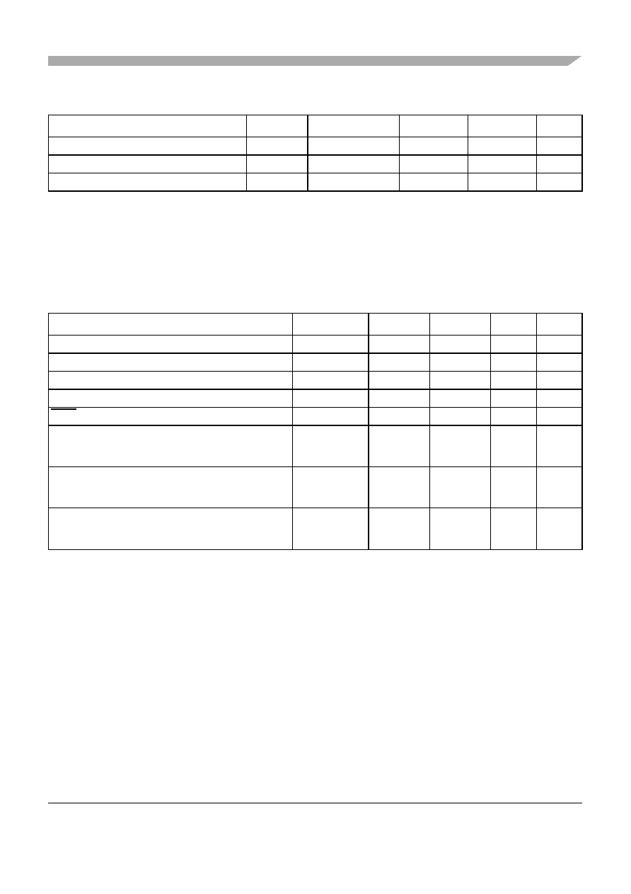
JTAG
21.2
JTAG AC Electrical Characteristics
This section describes the AC electrical specifications for the IEEE Std. 1149.1 (JTAG) interface of the
MPC8309. The following table provides the JTAG AC timing specifications as defined in Figure 40
through Figure 43.
Input high voltage
VIH
—2.0
OVDD +0.3
V
Input low voltage
VIL
—–0.3
0.8
V
Input current
IIN
0 V
VIN OVDD
—±5
A
Table 54. JTAG AC Timing Specifications (Independent of SYS_CLK_IN)1
At recommended operating conditions (see Table 2).
Parameter
Symbol2
Min
Max
Unit
Notes
JTAG external clock frequency of operation
fJTG
033.3
MHz
—
JTAG external clock cycle time
t JTG
30
—
ns
—
JTAG external clock pulse width measured at 1.4 V
tJTKHKL
11
—
ns
—
JTAG external clock rise and fall times
tJTGR, tJTGF
02
ns
—
TRST assert time
tTRST
25
—
ns
3
Input setup times:
Boundary-scan data
TMS, TDI
tJTDVKH
tJTIVKH
4
—
ns
4
Input hold times:
Boundary-scan data
TMS, TDI
tJTDXKH
tJTIXKH
10
—
ns
4
Valid times:
Boundary-scan data
TDO
tJTKLDV
tJTKLOV
2
15
ns
5
Table 53. JTAG Interface DC Electrical Characteristics (continued)
Characteristic
Symbol
Condition
Min
Max
Unit
相關(guān)PDF資料 |
PDF描述 |
|---|---|
| MPC8313EVRAFF | 32-BIT, 333 MHz, MICROPROCESSOR, PBGA516 |
| MPC8313EVRAGD | 32-BIT, 400 MHz, MICROPROCESSOR, PBGA516 |
| MPC8313EZQAGDB | 32-BIT, 400 MHz, MICROPROCESSOR, PBGA516 |
| MPC8313VRAFF | 32-BIT, 333 MHz, MICROPROCESSOR, PBGA516 |
| MPC8313ECZQAGD | 32-BIT, 400 MHz, MICROPROCESSOR, PBGA516 |
相關(guān)代理商/技術(shù)參數(shù) |
參數(shù)描述 |
|---|---|
| MPC8309EC | 制造商:FREESCALE 制造商全稱:Freescale Semiconductor, Inc 功能描述:PowerQUICC II Pro Integrated Communications Processor Family Hardware Specifications |
| MPC8309-KIT | 功能描述:開(kāi)發(fā)板和工具包 - 其他處理器 For MPC8309 Ethernet USB I2C SPI RoHS:否 制造商:Freescale Semiconductor 產(chǎn)品:Development Systems 工具用于評(píng)估:P3041 核心:e500mc 接口類型:I2C, SPI, USB 工作電源電壓: |
| MPC8309-KIT | 制造商:Freescale Semiconductor 功能描述:MPC830x Processor Evaluation Kit |
| MPC8309-SOM | 功能描述:開(kāi)發(fā)板和工具包 - 其他處理器 For MPC8309 Ethernet USB 16bit 32bit RoHS:否 制造商:Freescale Semiconductor 產(chǎn)品:Development Systems 工具用于評(píng)估:P3041 核心:e500mc 接口類型:I2C, SPI, USB 工作電源電壓: |
| MPC8309VMADDC | 制造商:Freescale Semiconductor 功能描述:MPC8309VMADDC - Bulk |
發(fā)布緊急采購(gòu),3分鐘左右您將得到回復(fù)。