- 您現(xiàn)在的位置:買賣IC網(wǎng) > PDF目錄69036 > MPC7410RX500LX (MOTOROLA INC) 32-BIT, 500 MHz, RISC PROCESSOR, CBGA360 PDF資料下載
參數(shù)資料
| 型號(hào): | MPC7410RX500LX |
| 廠商: | MOTOROLA INC |
| 元件分類: | 微控制器/微處理器 |
| 英文描述: | 32-BIT, 500 MHz, RISC PROCESSOR, CBGA360 |
| 封裝: | 25 X 25 MM, 3.20 MM HEIGHT, 1.27 MM PITCH, CERAMIC, BGA-360 |
| 文件頁數(shù): | 8/44頁 |
| 文件大小: | 885K |
| 代理商: | MPC7410RX500LX |
第1頁第2頁第3頁第4頁第5頁第6頁第7頁當(dāng)前第8頁第9頁第10頁第11頁第12頁第13頁第14頁第15頁第16頁第17頁第18頁第19頁第20頁第21頁第22頁第23頁第24頁第25頁第26頁第27頁第28頁第29頁第30頁第31頁第32頁第33頁第34頁第35頁第36頁第37頁第38頁第39頁第40頁第41頁第42頁第43頁第44頁
16
MPC7410 RISC Microprocessor Hardware Specifications
PRELIMINARY—SUBJECT TO CHANGE WITHOUT NOTICE
Electrical and Thermal Characteristics
1.4.2.3 L2 Clock AC Specifications
The L2CLK frequency is programmed by the L2 Configuration Register (L2CR[4:6]) core-to-L2 divisor
ratio. See Table 15 for example core and L2 frequencies at various divisors. Table 10 provides the potential
range of L2CLK output AC timing specifications as defined in Figure 7.
The L2SYNC_OUT signal is intended to be routed halfway out to the SRAMs and then returned to the
L2SYNC_IN input of the MPC7410 to synchronize L2CLKOUT at the SRAM with the processor’s internal
clock. L2CLKOUT at the SRAM can be offset forward or backward in time by shortening or lengthening
the routing of L2SYNC_OUT to L2SYNC_IN. See Motorola Application Note AN179/D “PowerPC
Backside L2 Timing Analysis for the PCB Design Engineer.”
The minimum L2CLK frequency of Table 10 is specified by the maximum delay of the internal DLL. The
variable-tap DLL introduces up to a full clock period delay in the L2CLKOUTA, L2CLKOUTB, and
L2SYNC_OUT signals so that the returning L2SYNC_IN signal is phase aligned with the next core clock
(divided by the L2 divisor ratio). Do not choose a core-to-L2 divisor which results in an L2 frequency below
this minimum, or the L2CLKOUT signals provided for SRAM clocking will not be phase aligned with the
MPC7410 core clock at the SRAMs.
The maximum L2CLK frequency shown in Table 10 is the core frequency divided by one. Very few L2
SRAM designs will be able to operate in this mode. Most designs will select a greater core-to-L2 divisor to
provide a longer L2CLK period for read and write access to the L2 SRAMs. The maximum L2CLK
frequency for any application of the MPC7410 will be a function of the AC timings of the MPC7410, the
AC timings for the SRAM, bus loading, and printed circuit board trace length.
Motorola is similarly limited by system constraints and cannot perform tests of the L2 interface on a
socketed part on a functional tester at the maximum frequencies of Table 10. Therefore, functional operation
and AC timing information are tested at core-to-L2 divisors of two or greater.
L2 input and output signals are latched or enabled, respectively, by the internal L2CLK (which is SYSCLK
multiplied up to the core frequency and divided down to the L2CLK frequency). In other words, the AC
timings of Table 11 are entirely independent of L2SYNC_IN. In a closed loop system, where L2SYNC_IN
is driven through the board trace by L2SYNC_OUT, L2SYNC_IN only controls the output phase of
L2CLKOUTA and L2CLKOUTB which are used to latch or enable data at the SRAMs. However, since in
a closed loop system L2SYNC_IN is held in phase alignment with the internal L2CLK, the signals of
Table 11 are referenced to this signal rather than the not-externally-visible internal L2CLK. During
manufacturing test, these times are actually measured relative to SYSCLK.
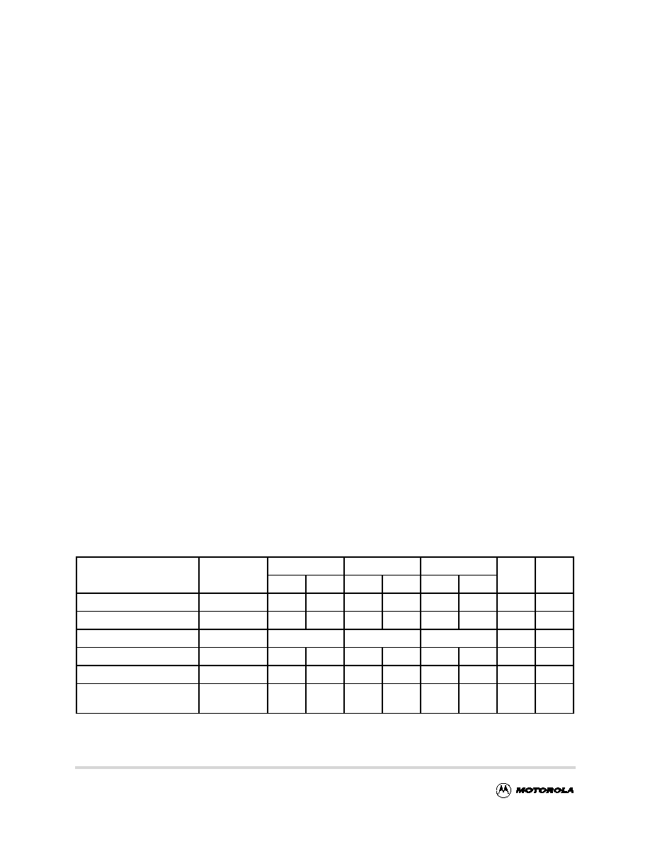
Table 10. L2CLK Output AC Timing Specifications
At recommended operating conditions (See Table 3)
Parameter
Symbol
400 MHz
450 MHz
500 MHz
Unit
Notes
Min
Max
Min
Max
Min
Max
L2CLK frequency
fL2CLK
133
400
133
400
133
400
MHz
1,4
L2CLK cycle time
tL2CLK
2.5
7.5
2.5
7.5
2.5
7.5
ns
L2CLK duty cycle
tCHCL/tL2CLK
50
%
2
Internal DLL-relock time
640
—
640
—
640
—
L2CLK
3
DLL capture window
010010010
ns
5
L2CLKOUT
output-to-output skew
tL2CSKW
—50
—
50
—50
ps
6
相關(guān)PDF資料 |
PDF描述 |
|---|---|
| MPC7410RX450LX | 32-BIT, 450 MHz, RISC PROCESSOR, CBGA360 |
| MPC8241LZP200X | 32-BIT, 200 MHz, RISC PROCESSOR, PBGA357 |
| MPC8245LZU350B | 32-BIT, 350 MHz, RISC PROCESSOR, PBGA352 |
| MPC8245LZU333B | 32-BIT, 333 MHz, RISC PROCESSOR, PBGA352 |
| MPC8245LZU300B | 32-BIT, 300 MHz, RISC PROCESSOR, PBGA352 |
相關(guān)代理商/技術(shù)參數(shù) |
參數(shù)描述 |
|---|---|
| MPC7410THX400LE | 功能描述:微處理器 - MPU NT HITCE RV1.4 1.8V -40C RoHS:否 制造商:Atmel 處理器系列:SAMA5D31 核心:ARM Cortex A5 數(shù)據(jù)總線寬度:32 bit 最大時(shí)鐘頻率:536 MHz 程序存儲(chǔ)器大小:32 KB 數(shù)據(jù) RAM 大小:128 KB 接口類型:CAN, Ethernet, LIN, SPI,TWI, UART, USB 工作電源電壓:1.8 V to 3.3 V 最大工作溫度:+ 85 C 安裝風(fēng)格:SMD/SMT 封裝 / 箱體:FBGA-324 |
| MPC7410THX400NE | 制造商:Freescale Semiconductor 功能描述:MPU MPC74XX RISC 64BIT 0.18UM 400MHZ 1.8V/2.5V/3.3V 360FCCBG - Bulk |
| MPC7410THX450NE | 功能描述:微處理器 - MPU NT NITCE RV1.4,1.8V -40C RoHS:否 制造商:Atmel 處理器系列:SAMA5D31 核心:ARM Cortex A5 數(shù)據(jù)總線寬度:32 bit 最大時(shí)鐘頻率:536 MHz 程序存儲(chǔ)器大小:32 KB 數(shù)據(jù) RAM 大小:128 KB 接口類型:CAN, Ethernet, LIN, SPI,TWI, UART, USB 工作電源電壓:1.8 V to 3.3 V 最大工作溫度:+ 85 C 安裝風(fēng)格:SMD/SMT 封裝 / 箱體:FBGA-324 |
| MPC7410THX500LE | 功能描述:微處理器 - MPU NT HITCE RV1.4 1.8V -40C RoHS:否 制造商:Atmel 處理器系列:SAMA5D31 核心:ARM Cortex A5 數(shù)據(jù)總線寬度:32 bit 最大時(shí)鐘頻率:536 MHz 程序存儲(chǔ)器大小:32 KB 數(shù)據(jù) RAM 大小:128 KB 接口類型:CAN, Ethernet, LIN, SPI,TWI, UART, USB 工作電源電壓:1.8 V to 3.3 V 最大工作溫度:+ 85 C 安裝風(fēng)格:SMD/SMT 封裝 / 箱體:FBGA-324 |
| MPC7410TRX400NE | 制造商:FREESCALE 制造商全稱:Freescale Semiconductor, Inc 功能描述:RISC Microprocessor Hardware Specifications Addendum |
發(fā)布緊急采購,3分鐘左右您將得到回復(fù)。