- 您現(xiàn)在的位置:買(mǎi)賣(mài)IC網(wǎng) > PDF目錄98013 > MCZ33781EK (FREESCALE SEMICONDUCTOR INC) SPECIALTY MICROPROCESSOR CIRCUIT, PDSO32 PDF資料下載
參數(shù)資料
| 型號(hào): | MCZ33781EK |
| 廠商: | FREESCALE SEMICONDUCTOR INC |
| 元件分類(lèi): | 微控制器/微處理器 |
| 英文描述: | SPECIALTY MICROPROCESSOR CIRCUIT, PDSO32 |
| 封裝: | 0.65 MM, LEAD FREE, SOIC-32 |
| 文件頁(yè)數(shù): | 10/44頁(yè) |
| 文件大小: | 940K |
| 代理商: | MCZ33781EK |
第1頁(yè)第2頁(yè)第3頁(yè)第4頁(yè)第5頁(yè)第6頁(yè)第7頁(yè)第8頁(yè)第9頁(yè)當(dāng)前第10頁(yè)第11頁(yè)第12頁(yè)第13頁(yè)第14頁(yè)第15頁(yè)第16頁(yè)第17頁(yè)第18頁(yè)第19頁(yè)第20頁(yè)第21頁(yè)第22頁(yè)第23頁(yè)第24頁(yè)第25頁(yè)第26頁(yè)第27頁(yè)第28頁(yè)第29頁(yè)第30頁(yè)第31頁(yè)第32頁(yè)第33頁(yè)第34頁(yè)第35頁(yè)第36頁(yè)第37頁(yè)第38頁(yè)第39頁(yè)第40頁(yè)第41頁(yè)第42頁(yè)第43頁(yè)第44頁(yè)

Analog Integrated Circuit Device Data
18
Freescale Semiconductor
33781
FUNCTIONAL DESCRIPTIONS
FUNCTIONAL INTERNAL BLOCK DESCRIPTION
VSUPn VOLTAGE MONITOR
This function monitors the voltage on the VSUPn pin. If the
voltage on the pin drops below the defined voltage threshold
for longer than the voltage threshold mask time, the 33781
will continue to send queued DBUS commands, but not set
any RNE bits in the DnSTAT registers to 1, until either the
device is reset by the RST pin or the EN bits in the DnEN
registers are first set to zero, and then to one (disabled and
then enabled). By monitoring the RNE bits the MCU will know
that communications have been disrupted and can take the
appropriate action.
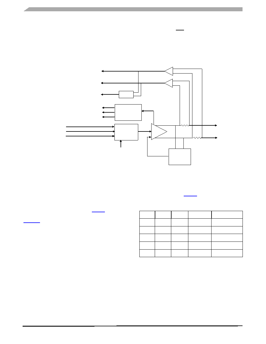
Figure 11. Driver/Receiver Block Diagram
DBUS DRIVER /RECEIVER (PHYSICAL LAYER)
There are four independent differential bus driver/receiver
blocks on the 33781. These blocks translate the transmit data
to the voltage and current needed to drive the DBUS. They
also detect the response current from the slave devices and
translate that current into digital levels. These circuits can
drive their outputs to the levels listed in Table 5.
The DBUS driver/receiver block diagram is shown in
Figure 11. The circuit uses a common driver for both the Idle
and Signal modes to minimize common mode noise. The
drivers are disabled in HiZ.
During Idle mode the driver is required to supply a high
current to recharge the Slave device storage capacitors. In
both Idle and Signal modes it is required to drive the DBUS
load capacitances and control the slew rate over a wide
supply voltage range and load conditions. Current limit, over-
current shutdown and thermal shutdown are included to
protect the device from fault conditions. More information can
be found in the Protection and Diagnostic Features and SPI0
Register and Bit Descriptions sections.
To ensure stability of the bus drivers, capacitors must be
connected between each output and ground. These are the
DBUS common mode capacitors. In addition, a bypass
capacitor is required at VSUPn. These capacitors must be
located close to the IC Pins and provide a low-impedance
path to ground.
The internal signal DSIF controls the Idle to Signalling
state change, and internal signal DSIS controls the signal
level, high or low. DSIR is the slave device response signal to
the logic. This is shown in Table 6.
Bus wire faults on a bus do not disrupt communications on
another bus. In addition, each bus channel has independent
thermal shutdown protection. Once the channel thermal limit
is reached the bus drivers become high-impedance, the TS
bit is set to a 1 and the EN bit set to 0 in the channel DEN
register. In addition the channel address buffer registers and
pointers are reset. There is a 4 usec filter on Tlim to prevent
false triggering.
The Differential Signal Generation block converts the
DSIS signal to the DBUS differential signal voltage levels.
This differential signal is buffered and slew rate controlled by
Differential
Signal
Generation
DSISn
DSIFn
hiZn
Common
Mode
Correction
Adder
Receiver Low n
Receiver High n
Receiver Sum n
Over Current
Over Temp
Sense
Signal Mode Over Current n
Idle Mode Over Current n
Over Temp n
DnH
DnL
Driver
Overvoltage
Over-current
Over-temp n
Over-temp
Over-voltage
Over-current
Receiver Low n
Receiver High n
Receiver Sum n
Sense
Adder
DSISn
DSIFn
hiZn
Differential
Signal
Generation
Common
Mode
Correction
DnH
DnL
Idle Mode Over-current n
Signal Mode Over-current n
Over-temp n
Driver
Table 6. Internal Signal Truth Table
DSIF
DSIS
TS
DSIR
DnD
0
Return Data
Signal Low
0
1
0
Return Data
Signal High
1
0
High-impedance
11
0
Idle
X
1
0
High-impedance
相關(guān)PDF資料 |
PDF描述 |
|---|---|
| MD1802FH | 10 A, 700 V, NPN, Si, POWER TRANSISTOR, TO-220AB |
| MD1802FX | 10 A, 700 V, NPN, Si, POWER TRANSISTOR |
| MD1803DFH | 10 A, 700 V, NPN, Si, POWER TRANSISTOR, TO-220AB |
| MD2001FX | 12 A, 700 V, NPN, Si, POWER TRANSISTOR |
| MD2103DFX | 6 A, 700 V, NPN, Si, POWER TRANSISTOR |
相關(guān)代理商/技術(shù)參數(shù) |
參數(shù)描述 |
|---|---|
| MCZ33781EKR2 | 功能描述:輸入/輸出控制器接口集成電路 DBUS2 MASTER STND RoHS:否 制造商:Silicon Labs 產(chǎn)品: 輸入/輸出端數(shù)量: 工作電源電壓: 最大工作溫度:+ 85 C 最小工作溫度:- 40 C 安裝風(fēng)格:SMD/SMT 封裝 / 箱體:QFN-64 封裝:Tray |
| MCZ33784EF | 功能描述:加速計(jì) - 板上安裝 DBUS2 SENSOR INTERFACE RoHS:否 制造商:Murata 傳感軸:Double 加速:12 g 靈敏度: 封裝 / 箱體: 輸出類(lèi)型:Analog 數(shù)字輸出 - 位數(shù):11 bit 電源電壓-最大:5.25 V 電源電壓-最小:4.75 V 電源電流:4 mA 最大工作溫度:+ 125 C 最小工作溫度:- 40 C |
| MCZ33784EF/R2- | 制造商:FREESCALE 制造商全稱(chēng):Freescale Semiconductor, Inc 功能描述:DSI 2.02 Sensor Interface |
| MCZ33784EFR2 | 功能描述:加速計(jì) - 板上安裝 DBUS2 SENSOR INTERFACE RoHS:否 制造商:Murata 傳感軸:Double 加速:12 g 靈敏度: 封裝 / 箱體: 輸出類(lèi)型:Analog 數(shù)字輸出 - 位數(shù):11 bit 電源電壓-最大:5.25 V 電源電壓-最小:4.75 V 電源電流:4 mA 最大工作溫度:+ 125 C 最小工作溫度:- 40 C |
| MCZ33789AE | 功能描述:網(wǎng)絡(luò)控制器與處理器 IC Airbag ASSP RoHS:否 制造商:Micrel 產(chǎn)品:Controller Area Network (CAN) 收發(fā)器數(shù)量: 數(shù)據(jù)速率: 電源電流(最大值):595 mA 最大工作溫度:+ 85 C 安裝風(fēng)格:SMD/SMT 封裝 / 箱體:PBGA-400 封裝:Tray |
發(fā)布緊急采購(gòu),3分鐘左右您將得到回復(fù)。