- 您現(xiàn)在的位置:買賣IC網(wǎng) > PDF目錄45234 > MC68HC2681P (FREESCALE SEMICONDUCTOR INC) 2 CHANNEL(S), 1M bps, SERIAL COMM CONTROLLER, PDIP40 PDF資料下載
參數(shù)資料
| 型號(hào): | MC68HC2681P |
| 廠商: | FREESCALE SEMICONDUCTOR INC |
| 元件分類: | 微控制器/微處理器 |
| 英文描述: | 2 CHANNEL(S), 1M bps, SERIAL COMM CONTROLLER, PDIP40 |
| 封裝: | PLASTIC, DIP-40 |
| 文件頁(yè)數(shù): | 29/88頁(yè) |
| 文件大?。?/td> | 726K |
| 代理商: | MC68HC2681P |
第1頁(yè)第2頁(yè)第3頁(yè)第4頁(yè)第5頁(yè)第6頁(yè)第7頁(yè)第8頁(yè)第9頁(yè)第10頁(yè)第11頁(yè)第12頁(yè)第13頁(yè)第14頁(yè)第15頁(yè)第16頁(yè)第17頁(yè)第18頁(yè)第19頁(yè)第20頁(yè)第21頁(yè)第22頁(yè)第23頁(yè)第24頁(yè)第25頁(yè)第26頁(yè)第27頁(yè)第28頁(yè)當(dāng)前第29頁(yè)第30頁(yè)第31頁(yè)第32頁(yè)第33頁(yè)第34頁(yè)第35頁(yè)第36頁(yè)第37頁(yè)第38頁(yè)第39頁(yè)第40頁(yè)第41頁(yè)第42頁(yè)第43頁(yè)第44頁(yè)第45頁(yè)第46頁(yè)第47頁(yè)第48頁(yè)第49頁(yè)第50頁(yè)第51頁(yè)第52頁(yè)第53頁(yè)第54頁(yè)第55頁(yè)第56頁(yè)第57頁(yè)第58頁(yè)第59頁(yè)第60頁(yè)第61頁(yè)第62頁(yè)第63頁(yè)第64頁(yè)第65頁(yè)第66頁(yè)第67頁(yè)第68頁(yè)第69頁(yè)第70頁(yè)第71頁(yè)第72頁(yè)第73頁(yè)第74頁(yè)第75頁(yè)第76頁(yè)第77頁(yè)第78頁(yè)第79頁(yè)第80頁(yè)第81頁(yè)第82頁(yè)第83頁(yè)第84頁(yè)第85頁(yè)第86頁(yè)第87頁(yè)第88頁(yè)
Programming and Register Descriptions
MOTOROLA
MC68HC681 USER’S MANUAL
4-5
4
Table 4-4 summarizes the various clock sources that can be selected for the counter/
timer.
Customers should use caution if the contents of a register are changed during receiver/
transmitter operation as certain changes can produce undesired results. For example,
changing the number of bits per character while the transmitter is active can transmit an
incorrect character. The contents of the clock-select register (CSR) and bit 7 of the
auxiliary control register (ACR[7]) should only be changed after the receiver(s) and
transmitter(s) have been issued software Rx and Tx reset commands. Most bits of the
mode registers should not be changed during receiver/transmitter operation, except that
in multidrop parity mode, the address/data parity type bit can be changed at any time.
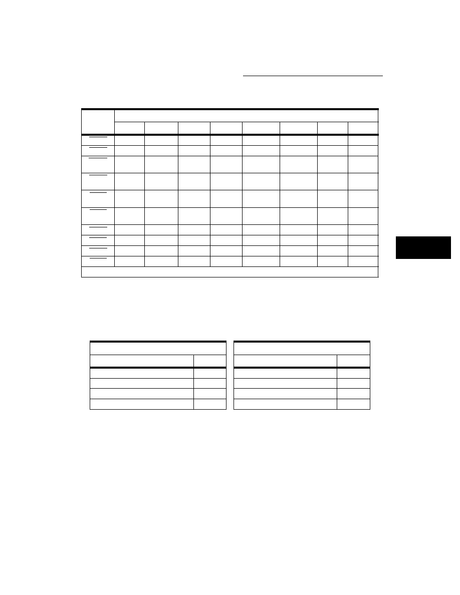
TxRDYA
OPCR[6] = 1*
TxRDYB
OPCR[7] = 1*
RxRDYA
OPCR[4] = 1
MR1A[6] = 0*
RxRDYB
OPCR[5] = 1
MR1B[6] = 0*
FFULLA
OPCR[4] = 1,
MR1A[6] = 1*
FFULLB
OPCR[5] = 1
MR1B[6] = 1*
RxRTRA
MR1A[7] = 1
TxRTSA
MR2A[5] = 1
RxRTRB
MR1B[7] = 1
TxRTSB
MR2B[5] = 1
NOTE:
The pin requires a pull-up resistor.
Table 4-4. Selection of Clock Sources for the Counter/Timer
ACR[6] = 0 (COUNTER MODE)
ACR[6] = 1 (TIMER MODE)
COUNTER MODE CLOCK SOURCES
ACR[5:4] =
TIMER MODE CLOCK SOURCES
ACR[5:4] =
Input Port Pin IP2
00
Input Port Pin IP2
00
Channel A 1X Transmitter Clock TxCA
01
Input Port Pin IP2 Divided by 16
01
Channel B 1X Transmitter Clock TxCB
10
Crystal/Clock X1
10
Crystal/Clock X1 Divided by 16
11
Crystal/Clock X1 Divided by 16
11
Table 4-3. Programming of Output Port Functions (Continued)
FUNCTION
OUTPUT PORT PIN
OP7
OP6
OP5
OP4
OP3
OP2
OP1
OP0
F
re
e
sc
a
le
S
e
m
ic
o
n
d
u
c
to
r,
I
Freescale Semiconductor, Inc.
For More Information On This Product,
Go to: www.freescale.com
n
c
..
.
相關(guān)PDF資料 |
PDF描述 |
|---|---|
| MC68HC2681P | 2 CHANNEL(S), 1M bps, SERIAL COMM CONTROLLER, PDIP40 |
| MC68HC681FN | 2 CHANNEL(S), 1M bps, SERIAL COMM CONTROLLER, PQCC44 |
| MC68HC681P | 2 CHANNEL(S), 1M bps, SERIAL COMM CONTROLLER, PDIP40 |
| MC68HC58FN | 1 CHANNEL(S), LOCAL AREA NETWORK CONTROLLER, PQCC28 |
| MC68HC58DW | 1 CHANNEL(S), LOCAL AREA NETWORK CONTROLLER, PDSO28 |
相關(guān)代理商/技術(shù)參數(shù) |
參數(shù)描述 |
|---|---|
| MC68HC34P | 制造商:Motorola Inc 功能描述: 制造商:Motorola Inc 功能描述:Static RAM, 256x8, 40 Pin, Plastic, DIP |
| MC68HC68T1P | 制造商:Motorola Inc 功能描述: |
| MC68HC705B16CFN | 制造商:Motorola Inc 功能描述: |
| MC68HC705B16FN | 制造商:Rochester Electronics LLC 功能描述: |
| MC68HC705B16NB | 制造商:Rochester Electronics LLC 功能描述: |
發(fā)布緊急采購(gòu),3分鐘左右您將得到回復(fù)。