- 您現(xiàn)在的位置:買賣IC網(wǎng) > PDF目錄371047 > MC68HC08AS32AVFU (MOTOROLA INC) Microcontrollers PDF資料下載
參數(shù)資料
| 型號(hào): | MC68HC08AS32AVFU |
| 廠商: | MOTOROLA INC |
| 元件分類: | 微控制器/微處理器 |
| 英文描述: | Microcontrollers |
| 中文描述: | 8-BIT, MROM, 8.4 MHz, MICROCONTROLLER, PQFP64 |
| 封裝: | QFP-64 |
| 文件頁(yè)數(shù): | 162/296頁(yè) |
| 文件大小: | 2291K |
| 代理商: | MC68HC08AS32AVFU |
第1頁(yè)第2頁(yè)第3頁(yè)第4頁(yè)第5頁(yè)第6頁(yè)第7頁(yè)第8頁(yè)第9頁(yè)第10頁(yè)第11頁(yè)第12頁(yè)第13頁(yè)第14頁(yè)第15頁(yè)第16頁(yè)第17頁(yè)第18頁(yè)第19頁(yè)第20頁(yè)第21頁(yè)第22頁(yè)第23頁(yè)第24頁(yè)第25頁(yè)第26頁(yè)第27頁(yè)第28頁(yè)第29頁(yè)第30頁(yè)第31頁(yè)第32頁(yè)第33頁(yè)第34頁(yè)第35頁(yè)第36頁(yè)第37頁(yè)第38頁(yè)第39頁(yè)第40頁(yè)第41頁(yè)第42頁(yè)第43頁(yè)第44頁(yè)第45頁(yè)第46頁(yè)第47頁(yè)第48頁(yè)第49頁(yè)第50頁(yè)第51頁(yè)第52頁(yè)第53頁(yè)第54頁(yè)第55頁(yè)第56頁(yè)第57頁(yè)第58頁(yè)第59頁(yè)第60頁(yè)第61頁(yè)第62頁(yè)第63頁(yè)第64頁(yè)第65頁(yè)第66頁(yè)第67頁(yè)第68頁(yè)第69頁(yè)第70頁(yè)第71頁(yè)第72頁(yè)第73頁(yè)第74頁(yè)第75頁(yè)第76頁(yè)第77頁(yè)第78頁(yè)第79頁(yè)第80頁(yè)第81頁(yè)第82頁(yè)第83頁(yè)第84頁(yè)第85頁(yè)第86頁(yè)第87頁(yè)第88頁(yè)第89頁(yè)第90頁(yè)第91頁(yè)第92頁(yè)第93頁(yè)第94頁(yè)第95頁(yè)第96頁(yè)第97頁(yè)第98頁(yè)第99頁(yè)第100頁(yè)第101頁(yè)第102頁(yè)第103頁(yè)第104頁(yè)第105頁(yè)第106頁(yè)第107頁(yè)第108頁(yè)第109頁(yè)第110頁(yè)第111頁(yè)第112頁(yè)第113頁(yè)第114頁(yè)第115頁(yè)第116頁(yè)第117頁(yè)第118頁(yè)第119頁(yè)第120頁(yè)第121頁(yè)第122頁(yè)第123頁(yè)第124頁(yè)第125頁(yè)第126頁(yè)第127頁(yè)第128頁(yè)第129頁(yè)第130頁(yè)第131頁(yè)第132頁(yè)第133頁(yè)第134頁(yè)第135頁(yè)第136頁(yè)第137頁(yè)第138頁(yè)第139頁(yè)第140頁(yè)第141頁(yè)第142頁(yè)第143頁(yè)第144頁(yè)第145頁(yè)第146頁(yè)第147頁(yè)第148頁(yè)第149頁(yè)第150頁(yè)第151頁(yè)第152頁(yè)第153頁(yè)第154頁(yè)第155頁(yè)第156頁(yè)第157頁(yè)第158頁(yè)第159頁(yè)第160頁(yè)第161頁(yè)當(dāng)前第162頁(yè)第163頁(yè)第164頁(yè)第165頁(yè)第166頁(yè)第167頁(yè)第168頁(yè)第169頁(yè)第170頁(yè)第171頁(yè)第172頁(yè)第173頁(yè)第174頁(yè)第175頁(yè)第176頁(yè)第177頁(yè)第178頁(yè)第179頁(yè)第180頁(yè)第181頁(yè)第182頁(yè)第183頁(yè)第184頁(yè)第185頁(yè)第186頁(yè)第187頁(yè)第188頁(yè)第189頁(yè)第190頁(yè)第191頁(yè)第192頁(yè)第193頁(yè)第194頁(yè)第195頁(yè)第196頁(yè)第197頁(yè)第198頁(yè)第199頁(yè)第200頁(yè)第201頁(yè)第202頁(yè)第203頁(yè)第204頁(yè)第205頁(yè)第206頁(yè)第207頁(yè)第208頁(yè)第209頁(yè)第210頁(yè)第211頁(yè)第212頁(yè)第213頁(yè)第214頁(yè)第215頁(yè)第216頁(yè)第217頁(yè)第218頁(yè)第219頁(yè)第220頁(yè)第221頁(yè)第222頁(yè)第223頁(yè)第224頁(yè)第225頁(yè)第226頁(yè)第227頁(yè)第228頁(yè)第229頁(yè)第230頁(yè)第231頁(yè)第232頁(yè)第233頁(yè)第234頁(yè)第235頁(yè)第236頁(yè)第237頁(yè)第238頁(yè)第239頁(yè)第240頁(yè)第241頁(yè)第242頁(yè)第243頁(yè)第244頁(yè)第245頁(yè)第246頁(yè)第247頁(yè)第248頁(yè)第249頁(yè)第250頁(yè)第251頁(yè)第252頁(yè)第253頁(yè)第254頁(yè)第255頁(yè)第256頁(yè)第257頁(yè)第258頁(yè)第259頁(yè)第260頁(yè)第261頁(yè)第262頁(yè)第263頁(yè)第264頁(yè)第265頁(yè)第266頁(yè)第267頁(yè)第268頁(yè)第269頁(yè)第270頁(yè)第271頁(yè)第272頁(yè)第273頁(yè)第274頁(yè)第275頁(yè)第276頁(yè)第277頁(yè)第278頁(yè)第279頁(yè)第280頁(yè)第281頁(yè)第282頁(yè)第283頁(yè)第284頁(yè)第285頁(yè)第286頁(yè)第287頁(yè)第288頁(yè)第289頁(yè)第290頁(yè)第291頁(yè)第292頁(yè)第293頁(yè)第294頁(yè)第295頁(yè)第296頁(yè)
Input/Output (I/O) Ports
Data Sheet
MC68HC08AS32A — Rev. 1
162
Input/Output (I/O) Ports
MOTOROLA
pin. The data latch can always be written, regardless of the state of its data
direction bit.
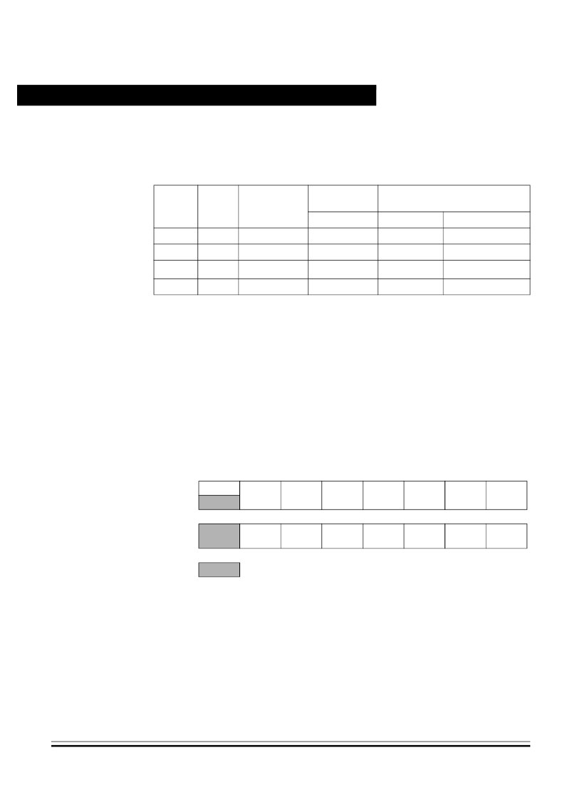
Table 12-3
summarizes the operation of the port C pins.
12.5 Port D
Port D is an 8-bit special-function I/O port that shares all of its pins with the
analog-to-digital converter (ADC).
12.5.1 Port D Data Register
The port D data register contains a data latch for the seven port D pins.
PTD[6:0] — Port D Data Bits
PTD[6:0] are read/write, software programmable bits. Data direction of PTD[6:0]
pins are under the control of the corresponding bit in data direction register D.
ATD[14:8] — ADC Channel Status Bits
PTD6/ATD14/TCLK–PTD0/ATD8 are seven of the 15 analog-to-digital
converter channels. The ADC channel select bits, CH[4:0], determine whether
the PTD6/ATD14/TCLK–PTD0/ATD8 pins are ADC channels or
general-purpose I/O pins. If an ADC channel is selected and a read of this
Table 12-3. Port C Pin Functions
DDRC
Bit
PTC
Bit
I/O Pin
Mode
Accesses
to DDRC
Accesses to PTC
Read/Write
Read
Write
[7] = 0
PTC2
Input, Hi-Z
DDRC[7]
0
PTC2
[7] = 1
PTC2
Output, MCLK
DDRC[7]
Data Latch
—
0
X
Input, Hi-Z
DDRC[4:0]
Pin
PTC[4:3, 1:0]
(1)
1
X
Output
DDRC[4:0]
PTC[4:0]
PTC[4:3, 1:0]
X = Don’t Care
Hi-Z = High Impedance
1. Writing affects data register, but does not affect input.
Address:
$0003
Bit 7
6
5
4
3
2
1
Bit 0
Read:
0
PTD6
PTD5
PTD4
PTD3
PTD2
PTD1
PTD0
Write:
Reset:
Unaffected by Reset
Alternate
Functions:
ATD14/
TCLK
ATD13
ATD12
ATD11
ATD10
ATD9
ATD8
= Unimplemented
Figure 12-11. Port D Data Register (PTD)
F
Freescale Semiconductor, Inc.
For More Information On This Product,
Go to: www.freescale.com
n
.
相關(guān)PDF資料 |
PDF描述 |
|---|---|
| MC68HC08AS32CAFN | Microcontrollers |
| MC68HC08AS32VAFN | Microcontrollers |
| MC68HC08AS32A | Microcontrollers |
| MC68HC08AS32ACFU | Microcontrollers |
| MC68HC08AS32AFN | Microcontrollers |
相關(guān)代理商/技術(shù)參數(shù) |
參數(shù)描述 |
|---|---|
| MC68HC08AZ0 | 制造商:MOTOROLA 制造商全稱:Motorola, Inc 功能描述:Advance Information |
| MC68HC08AZ0CFU | 制造商:MOTOROLA 制造商全稱:Motorola, Inc 功能描述:Advance Information |
| MC68HC08AZ16 | 制造商:MOTOROLA 制造商全稱:Motorola, Inc 功能描述:HCMOS Microcontroller Unit |
| MC68HC08AZ24 | 制造商:MOTOROLA 制造商全稱:Motorola, Inc 功能描述:HCMOS Microcontroller Unit |
| MC68HC08AZ32 | 制造商:FREESCALE 制造商全稱:Freescale Semiconductor, Inc 功能描述:Advance Information |
發(fā)布緊急采購(gòu),3分鐘左右您將得到回復(fù)。