- 您現(xiàn)在的位置:買賣IC網(wǎng) > PDF目錄378661 > MC44011FB (MOTOROLA INC) BUS CONTROLLED MULTISTANDARD VIDEO PROCESSOR PDF資料下載
參數(shù)資料
| 型號: | MC44011FB |
| 廠商: | MOTOROLA INC |
| 元件分類: | 消費家電 |
| 英文描述: | BUS CONTROLLED MULTISTANDARD VIDEO PROCESSOR |
| 中文描述: | SPECIALTY CONSUMER CIRCUIT, PQFP44 |
| 封裝: | PLASTIC, QFP-44 |
| 文件頁數(shù): | 33/52頁 |
| 文件大小: | 835K |
| 代理商: | MC44011FB |
第1頁第2頁第3頁第4頁第5頁第6頁第7頁第8頁第9頁第10頁第11頁第12頁第13頁第14頁第15頁第16頁第17頁第18頁第19頁第20頁第21頁第22頁第23頁第24頁第25頁第26頁第27頁第28頁第29頁第30頁第31頁第32頁當(dāng)前第33頁第34頁第35頁第36頁第37頁第38頁第39頁第40頁第41頁第42頁第43頁第44頁第45頁第46頁第47頁第48頁第49頁第50頁第51頁第52頁
MC44011
33
MOTOROLA ANALOG IC DEVICE DATA
Write to Control Registers
Writing should be done only during vertical retrace. A write
cycle consists of three bytes (with three acknowledge bits):
1) The first byte is always the write address for the
MC44011 ($8A).
2) The second byte defines the sub–address register
(within the MC44011) to be operated on ($77 through
$88, and $00).
3) The third byte is the data for that register.
Communication begins when a start bit (data taken low
while clock is high), initiated by the master, is detected,
generating an internal reset. The first byte is then entered,
and if the address is correct ($8A), an acknowledge is
generated by the MC44011, which tells the master to
continue the communication. The second byte is then
entered, followed by an acknowledge. The third byte is the
operative data which is directed to the designated register,
followed by a third acknowledge.
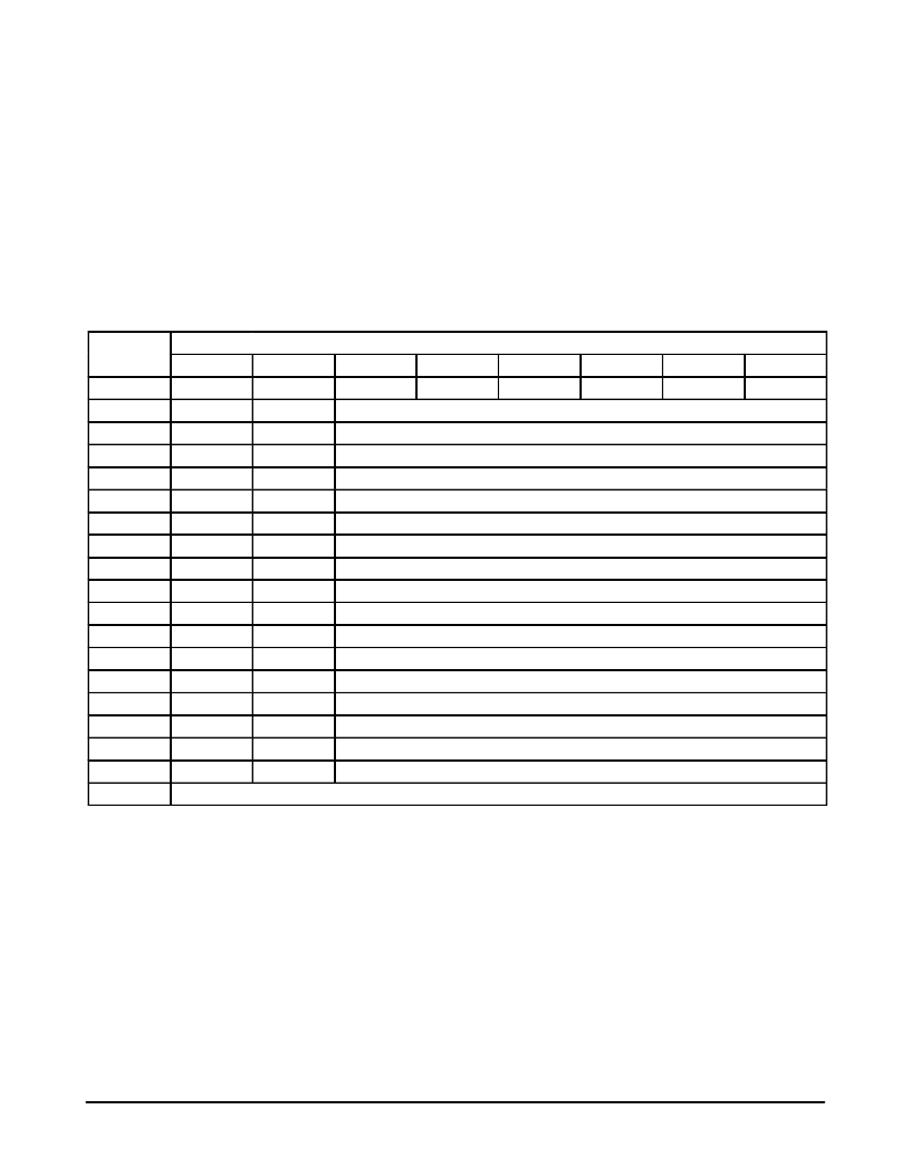
Sub–Address Registers
The sub–addresses of the 19 registers are at $77
through $88, and $00. Fourteen of the registers use Bits
0–5 to operate DACs which provide the analog
adjustments. Most of the other bits are used to set/reset
functions, and to select appropriate inputs/outputs. Table 13
indicates the assignments of the registers.
Table 13. Sub–Address Register Assignments
Sub–
Address
7
6
5
4
3
2
1
0
$77
S–VHS Y
S–VHS C
FSI
L2 GATE
BLCP
L1 GATE
CBI
CAI
$78
36/38
μ
s
Cal Kill
(R–Y)/(B–Y) adjust DAC
$79
HI
VI
Subcarrier balance DAC
$7A
Xtal
SSD
$7B
T1
T2
$7C
SSC
SSA
$7D
P1
SSB
Blue bias for YUV operation DAC
$7E
P3
P2
Red bias for YUV operation DAC
$7F
D3
D1
Pixel Clock VCO Gain adjust DAC
$80
RGB EN
D2
Blue Contrast trim DAC
$81
Y2 EN
Y1 EN
Main Contrast DAC
$82
YUV EN
YX EN
Red Contrast trim DAC
$83
L2 Gain
L1 Gain
Blue Brightness trim DAC
$84
H Switch
525/625
Main Brightness DAC
$85
PClk/2
C Sync
Red Brightness trim DAC
$86
Vin Sync
Y2 Sync
PLL1 En
Main Saturation DAC (Color Difference section )
$87
0
(R–Y)/(B–Y) Saturation balance DAC (Decoder section)
$88
V2/V1
RGB Sync
Hue DAC
$00
Set to $00 to start Horizontal Loop if $88–6 = 0
Table 14 is a brief explanation of the individual control bits.
A more detailed explanation of the functions is found in the
block diagram description of the text (within the Functional
Description section). Table 15 provides an explanation of the
DACs. Each DAC is 6 bits wide, allowing 64 adjustment
steps. The proper sequence and control of the bits and
DACs, to achieve various system functions, is described in
the Applications Information section.
相關(guān)PDF資料 |
PDF描述 |
|---|---|
| MC44011FN | BUS CONTROLLED MULTISTANDARD VIDEO PROCESSOR |
| MC44871DTB | PLL TUNING CIRCUIT WITH HIGH SPEED I2C BUS AND 30 V TUNING SUPPLY |
| MC68705P3CS | 8-Bit EPROM Microcomputer Unit |
| MC68705P3 | 8-Bit EPROM Microcomputer Unit |
| MC68705P3S | 8-Bit EPROM Microcomputer Unit |
相關(guān)代理商/技術(shù)參數(shù) |
參數(shù)描述 |
|---|---|
| MC44011FN | 制造商:MOTOROLA 制造商全稱:Motorola, Inc 功能描述:Chroma 4 Multistandard Video Processor |
| MC4403 | 制造商:SHENZHENFREESCALE 制造商全稱:ShenZhen FreesCale Electronics. Co., Ltd 功能描述:P-Channel 20-V (D-S) MOSFET High performance trench technology |
| MC44030FTB | 制造商:MOTOROLA 制造商全稱:Motorola, Inc 功能描述:MULTISTANDARD VIDEO SIGNAL PROCESSOR WITH INTEGRATED CHROMA DELAY LINE |
| MC44030P | 制造商:MOTOROLA 制造商全稱:Motorola, Inc 功能描述:MULTISTANDARD VIDEO SIGNAL PROCESSOR WITH INTEGRATED CHROMA DELAY LINE |
| MC44035FTB | 制造商:MOTOROLA 制造商全稱:Motorola, Inc 功能描述:MULTISTANDARD VIDEO SIGNAL PROCESSOR WITH INTEGRATED CHROMA DELAY LINE |
發(fā)布緊急采購,3分鐘左右您將得到回復(fù)。