- 您現(xiàn)在的位置:買賣IC網(wǎng) > PDF目錄369892 > MC100EP222 (Motorola, Inc.) Low Voltage ECL/PECL 1:15 Clock Driver(低壓ECL/PECL 1:15時鐘驅(qū)動器) PDF資料下載
參數(shù)資料
| 型號: | MC100EP222 |
| 廠商: | Motorola, Inc. |
| 英文描述: | Low Voltage ECL/PECL 1:15 Clock Driver(低壓ECL/PECL 1:15時鐘驅(qū)動器) |
| 中文描述: | 低壓ECL / PECL的一時15分時鐘驅(qū)動器(低壓ECL / PECL的一時15時鐘驅(qū)動器) |
| 文件頁數(shù): | 5/8頁 |
| 文件大小: | 151K |
| 代理商: | MC100EP222 |

5
Motorola
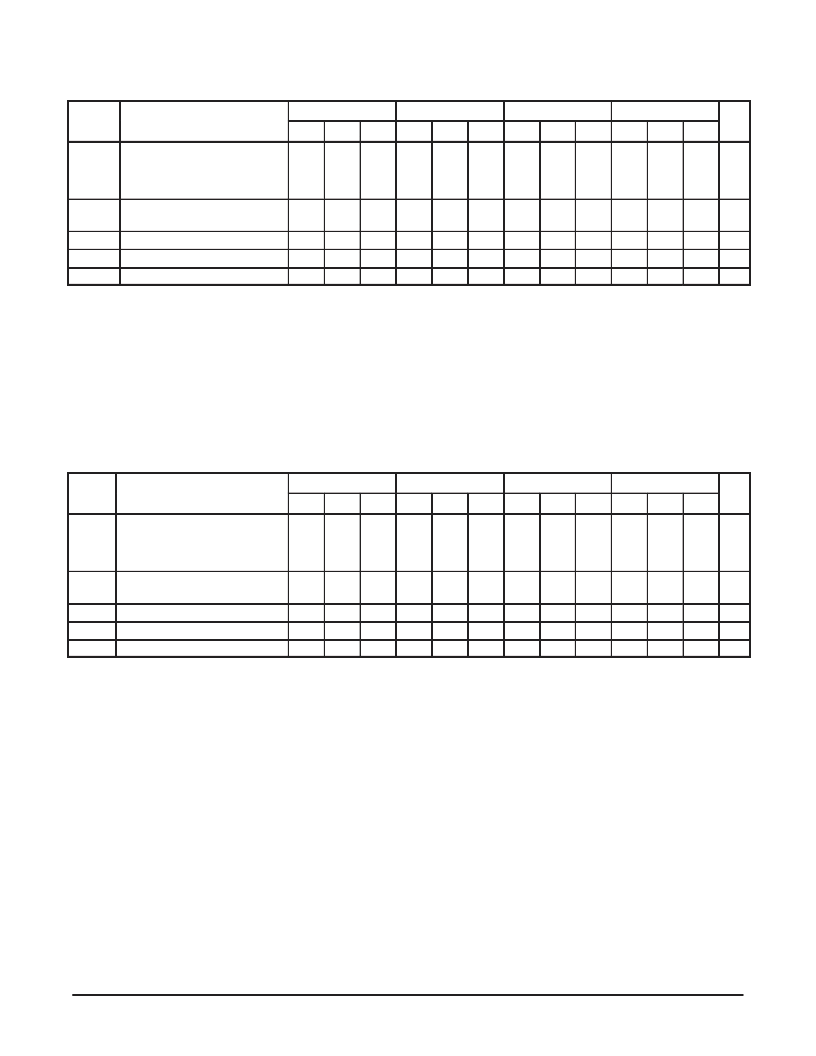
ECL AC CHARACTERISTICS
(V
EE
=V
EEmin
to V
EEmax
, V
CC
=V
CCO
=GND)
Symbol
Characteristics
-40 deg C
0 deg C
25 deg C
85 deg C
Unit
Min
Typ
Max
Min
Typ
Max
Min
Typ
Max
Min
Typ
Max
t
PD
Propagation Delay
CLK
N
to Q
XX
(differential)
a
CLK
N
to Q
XX
(single-ended)
b
MR to Q
XX
Pin-to-Pin Skew
c
Part-to-Part Skew
d
Minimum Input Swing
e
Common Mode Range
f
Output Rise/Fall Time
g
a. The differential propagation delay is defined as the delay from the crossing points of the differential input signal to the crossing point of the
differential output signal
b. The single ended propagation delay is defined as the delay from the 50% point of the input signal to the 50% point of the output signal
c. The pin-to-pin skew is defined as the worst case difference in propagation delay between any two similar delay path within a single device
d. Output-to-output skew is defined as the worst case difference in propagation delay between any output of any device operating under the
same conditions
e. V
PPmin
is defined as the minimum input differential voltage which will cause no increase of the propagation delay.
VPP
min
is AC limited. A differential input signal of 50 mV will still produce full ECL levels at the output.
f.
V
CMR
is defined as the range within the VIH level may vary, with the device still meeting the propagatio delay specification. The VIL level
must be such that the peak-to-peak voltage is less than 1.0 V and greater or equal to VPPmin.
g. 20%-80%
900
900
1000
900
900
1000
900
900
1000
900
900
1000
ps
t
SK(O)
t
SK(PP)
V
PP
V
CMR
t
r
, t
f
50
150
50
150
50
150
50
150
ps
400
400
400
400
mV
V
200
200
200
200
ps
PECL AC CHARACTERISTICS
(V
EE
=GND, V
CC
=V
CCO
=V
CCmin
to V
CCmax
)
Symbol
Characteristics
-40 deg C
0 deg C
25 deg C
85 deg C
Unit
Min
Typ
Max
Min
Typ
Max
Min
Typ
Max
Min
Typ
Max
t
PD
Propagation Delay
CLK
N
to Q
XX
(differential)
a
CLK
N
to Q
XX
(single-ended)
b
MR to Q
XX
Pin-to-Pin Skew
c
Part-to-Part Skew
Minimum Input Swing
d
Common Mode Range
e
Output Rise/Fall Time
f
a. The differential propagation delay is defined as the delay from the crossing points of the differential input signal to the crossing point of the
differential output signal
b. The single ended propagation delay is defined as the delay from the 50% point of the input signal to the 50% point of the output signal
c. The pin-to-pin skew is defined as the worst case difference between any two similar delay path within a single device
d. VPPmin is defined as the minimum input differential voltage which will cause no increase of the propagation delay. VPPmin is AC limited. A
differential input signal of 50 mV will still produce full ECL levels at the output.
e. V
CMR
is defined as the range within the VIH level may vary, with the device still meeting the propagation delay specification. The VIL level
must be such that the peak-to-peak voltage is less than 1.0 V and greater or equal to VPPmin.
f.
20%-80%
900
900
1000
900
900
1000
900
900
1000
900
900
1000
ps
t
sk(o)
t
sk(pp)
V
PP
V
CMR
t
r
/t
f
50
150
50
150
50
150
50
150
ps
400
400
400
400
mV
V
200
200
200
200
ps
相關(guān)PDF資料 |
PDF描述 |
|---|---|
| MC100EP223 | Low-Voltage 1:22 Differential PECL/HSTL Clock Driver(低壓1:22差分PECL/HSTL時鐘驅(qū)動器) |
| MC100H606FN | Registered Hex TTL/PECL Translator |
| MC10H606 | Registered Hex TTL/PECL Translator |
| MC10H606FN | Registered Hex TTL/PECL Translator |
| MC100H607FN | Registered Hex PECL/TTL Translator |
相關(guān)代理商/技術(shù)參數(shù) |
參數(shù)描述 |
|---|---|
| MC100EP223 | 制造商:MOTOROLA 制造商全稱:Motorola, Inc 功能描述:Low-Voltage 1:22 Differential PECL/HSTL Clock Driver |
| MC100EP223TC | 制造商:MOTOROLA 制造商全稱:Motorola, Inc 功能描述:Low-Voltage 1:22 Differential PECL/HSTL Clock Driver |
| MC100EP24D | 制造商:ON Semiconductor 功能描述: |
| MC100EP29 | 制造商:ONSEMI 制造商全稱:ON Semiconductor 功能描述:3.3V / 5V ECL Dual Differential Data and Clock D Flip−Flop With Set and Reset |
| MC100EP29DT | 功能描述:觸發(fā)器 3.3V/5V ECL Dual RoHS:否 制造商:Texas Instruments 電路數(shù)量:2 邏輯系列:SN74 邏輯類型:D-Type Flip-Flop 極性:Inverting, Non-Inverting 輸入類型:CMOS 輸出類型: 傳播延遲時間:4.4 ns 高電平輸出電流:- 16 mA 低電平輸出電流:16 mA 電源電壓-最大:5.5 V 最大工作溫度:+ 85 C 安裝風(fēng)格:SMD/SMT 封裝 / 箱體:X2SON-8 封裝:Reel |
發(fā)布緊急采購,3分鐘左右您將得到回復(fù)。