- 您現(xiàn)在的位置:買賣IC網(wǎng) > PDF目錄377878 > MB15F63ULPVA1 (FUJITSU LTD) Dual Serial Input PLL Frequency Synthesizer PDF資料下載
參數(shù)資料
| 型號(hào): | MB15F63ULPVA1 |
| 廠商: | FUJITSU LTD |
| 元件分類: | XO, clock |
| 英文描述: | Dual Serial Input PLL Frequency Synthesizer |
| 中文描述: | PLL FREQUENCY SYNTHESIZER, 2000 MHz, PQCC20 |
| 封裝: | 3.50 X 3.50 MM, 0.60 MM HEIGHT, LCC-20 |
| 文件頁數(shù): | 4/36頁 |
| 文件大小: | 231K |
| 代理商: | MB15F63ULPVA1 |
第1頁第2頁第3頁當(dāng)前第4頁第5頁第6頁第7頁第8頁第9頁第10頁第11頁第12頁第13頁第14頁第15頁第16頁第17頁第18頁第19頁第20頁第21頁第22頁第23頁第24頁第25頁第26頁第27頁第28頁第29頁第30頁第31頁第32頁第33頁第34頁第35頁第36頁
MB15F63UL
4
■
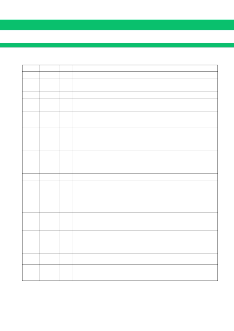
PIN DESCRIPTIONS
Pin no. Pin name
I/O
O
O
Descriptions
1
VPIF
Charge pump power supply for the IF-PLL
2
DoIF
Charge pump output for the IF-PLL
3
GND
Ground pin
4
SW
Open-drain switch pin for changing over the high-speed mode filter
5
DoRF
O
Charge pump output for the RF-PLL
6
VPRF
Power supply for the RF-PLL charge pump
7
LD/fout
O
Lock detect signal output (LD) /phase comparator monitoring output (fout) pin.
The output signal is selected by LDS bit in a serial data.
LDS bit
=
“H” : outputs fout signal/LDS bit
=
“L” : outputs LD signal
Power saving mode control for the RF-PLL section. This pin must be set at “L” when
the power supply is started up. (Open is prohibited. )
PS
=
“H” : Normal mode/PS
=
“L” : Power saving mode
Ground pin
8
PSRF
I
9
GND
10
XfinRF
I
Prescaler complimentary input pin for the RF-PLL section.
This pin should be grounded via a capacitor.
11
finRF
I
Prescaler input pin for the RF-PLL.
Connection to an external VCO should be via AC coupling.
12
VccRF
Power supply pin for the RF-PLL
13
LE
I
Load enable signal input pin (with the schmitt trigger circuit)
When LE is set “H”, data in the shift register is transferred to the corresponding latch
according to the control bit in a serial data.
14
Data
I
Serial data input pin (with the schmitt trigger circuit)
Data is transferred to the corresponding latch (IF-ref. counter, IF-prog. counter,
RF-ref. counter, RF-prog. counter) according to the control bit in a serial data.
15
CLK
I
Clock input pin for the 29-bit shift register (with the schmitt trigger circuit)
One bit data is shifted into the shift register on a rising edge of the clock.
16
VccIF
Power supply pin for the IF-PLL
17
OSCin
I
The programmable reference divider input pin. TCXO should be connected with an
AC coupling capacitor.
18
XfinIF
I
Prescaler complimentary input for the IF-PLL section.
This pin should be grounded via a capacitor.
19
finIF
I
Prescaler input pin for the IF-PLL.
Connection to an external VCO should be AC coupling.
20
PSIF
I
Power saving mode control pin for the IF-PLL section. This pin must be set at “L”
when the power supply is started up. (Open is prohibited.)
PS bit
=
“H” : Normal mode/PS bit
=
“L” : Power saving mode
相關(guān)PDF資料 |
PDF描述 |
|---|---|
| MB15F63UL | Dual Serial Input PLL Frequency Synthesizer |
| MB15F72UL | Dual Serial Input PLL Frequency Synthesizer |
| MB15F72ULPFT | Dual Serial Input PLL Frequency Synthesizer |
| MB15F72ULPVA | Dual Serial Input PLL Frequency Synthesizer |
| MB15F72UV | Dual Serial Input PLL Frequency Synthesizer |
相關(guān)代理商/技術(shù)參數(shù) |
參數(shù)描述 |
|---|---|
| MB15F63ULPVA1-GE1 | 制造商:Fujitsu 功能描述:Bulk |
| MB15F72SP | 制造商:FUJITSU 制造商全稱:Fujitsu Component Limited. 功能描述:Dual Serial Input PLL Frequency Synthesizer |
| MB15F72SPPFT | 制造商:FUJITSU 制造商全稱:Fujitsu Component Limited. 功能描述:Dual Serial Input PLL Frequency Synthesizer |
| MB15F72SPPV | 制造商:FUJITSU 制造商全稱:Fujitsu Component Limited. 功能描述:Dual Serial Input PLL Frequency Synthesizer |
| MB15F72UL | 制造商:FUJITSU 制造商全稱:Fujitsu Component Limited. 功能描述:Dual Serial Input PLL Frequency Synthesizer |
發(fā)布緊急采購,3分鐘左右您將得到回復(fù)。