- 您現(xiàn)在的位置:買賣IC網(wǎng) > PDF目錄377825 > M39432 (意法半導體) Single Chip 4Mbit Flash and 256Kbit Parallel EEPROM Memory(單片4Mb閃速和256Kb并行EEPROM) PDF資料下載
參數(shù)資料
| 型號: | M39432 |
| 廠商: | 意法半導體 |
| 英文描述: | Single Chip 4Mbit Flash and 256Kbit Parallel EEPROM Memory(單片4Mb閃速和256Kb并行EEPROM) |
| 中文描述: | 單芯片的4Mb并行閃存和256Kbit EEPROM存儲器(單片4Mb的閃速和256Kb的并行的EEPROM) |
| 文件頁數(shù): | 2/30頁 |
| 文件大小: | 247K |
| 代理商: | M39432 |
第1頁當前第2頁第3頁第4頁第5頁第6頁第7頁第8頁第9頁第10頁第11頁第12頁第13頁第14頁第15頁第16頁第17頁第18頁第19頁第20頁第21頁第22頁第23頁第24頁第25頁第26頁第27頁第28頁第29頁第30頁
Symbol
Parameter
Value
Unit
T
A
Ambient Operating Temperature
–40 to 85
°
C
T
BIAS
Temperature Under Bias
–50 to 125
°
C
T
STG
Storage Temperature
–65 to 150
°
C
V
IO (2)
Input or Output Voltages
–0.6 to 7
V
V
CC
Supply Voltage
–0.6 to 7
V
V
A9
, V
G
, V
EF (2)
A9, G, EF Voltage
–0.6 to 13.5
V
Notes:
1. Except for the rating "Operating Temperature Range", stresses above those listed in the Table "Absolute Maximum Ratings"
may cause permanent damage to the device. These are stress ratings only and operation of the device at these or any other
conditions above those indicated in the Operating sections of this specification is not implied. Exposure to Absolute Maximum
Rating conditions for extended periods may affect device reliability. Refer also to the STMicroelectronics SURE Program and other
relevant quality documents.
2. Minimum Voltage may undershoot to –2V during transition and for less than 20ns.
Table 2. Absolute Maximum Ratings
(1)
An additional 64 bytes of EPROM are One Time
Programmable.
DESCRIPTION
(Cont’d)
Warning:
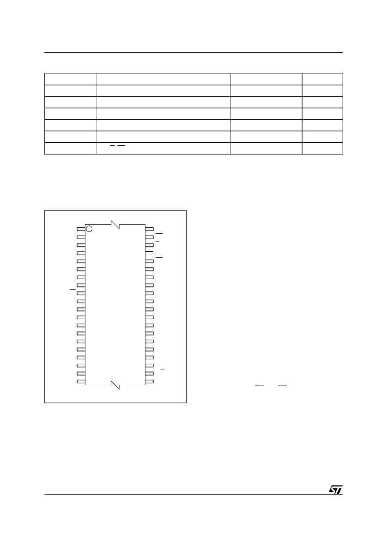
NC = Not Connected.
A3
R/B
NC
A0
A1
A2
DQ0
A7
A6
A5
NC
A4
NC
A13
A14
A17
W
VCC
EE
G
A10
EF
A11
A9
A8
NC
DQ7
DQ6
NC
VSS
DQ2
DQ5
DQ4
DQ1
DQ3
A16
A15
A12
A18
AI01947
M39432
10
11
1
20
21
30
31
40
NC
Figure 2. TSOP Pin Connections
The M39432 EEPROM array may be written by
byte or by page of 64 bytes and the integrity of the
data can be secured with the help of the Software
Data Protection (SDP).
The M39432 Flash Memory array offers 8 blocks of
64 Kbytes, each sector may be erased individually,
and programmed Byte-by-Byte. Each block can be
separately protected and unprotected against pro-
gram and erase. Block erasure may be suspended,
while data is read from other blocks of the Flash
array (or EEPROM memory block), and then re-
sumed. The Flash array is functionally compatible
with the M29W040 4 Mbit Single Voltage Flash
Memory.
During a Program or Erase cycle in the Flash array
or during a Write in the EEPROM memory block,
the status of the M39432 internal logic can be read
on the Data Outputs DQ7,DQ6, DQ5 and DQ3.
PIN DESCRIPTION
Address Inputs (A0-A18).
The address inputs for
the memory array are latched during a write opera-
tion. A0-A14 access locations in the EEPROM
memory block A0-A18 access locations in the Flash
memory block. The memory block selected is given
by the state on the EE and EF inputs respectively.
When a specific voltage (V
ID
) is applied on the A9
address input, additional specific areas can be
accessed: Read the Manufacturer identifier, Read
the Flash block identifier, Read/Write the EEPROM
block identifier, Verify the Flash Block Protection
Status.
2/30
M39432
相關(guān)PDF資料 |
PDF描述 |
|---|---|
| M40Z111MH6 | 5V OR 3V NVRAM SUPERVISOR FOR UP TO TWO LPSRAMs |
| M40Z111MH6TR | 5V OR 3V NVRAM SUPERVISOR FOR UP TO TWO LPSRAMs |
| M40Z111WMH6 | 5V OR 3V NVRAM SUPERVISOR FOR UP TO TWO LPSRAMs |
| M40Z111WMH6TR | 5V OR 3V NVRAM SUPERVISOR FOR UP TO TWO LPSRAMs |
| M40Z111 | NVRAM Controller for up to Two LPSRAM(NVRAM控制器) |
相關(guān)代理商/技術(shù)參數(shù) |
參數(shù)描述 |
|---|---|
| M39432-10VNC6T | 制造商:STMICROELECTRONICS 制造商全稱:STMicroelectronics 功能描述:Single Chip 4 Mbit Flash Memory and 256 Kbit Parallel EEPROM |
| M39432-10WNC6T | 制造商:STMICROELECTRONICS 制造商全稱:STMicroelectronics 功能描述:Single Chip 4 Mbit Flash Memory and 256 Kbit Parallel EEPROM |
| M39432-12VNC6T | 制造商:STMICROELECTRONICS 制造商全稱:STMicroelectronics 功能描述:Single Chip 4 Mbit Flash Memory and 256 Kbit Parallel EEPROM |
| M39432-12WNC6T | 制造商:STMICROELECTRONICS 制造商全稱:STMicroelectronics 功能描述:Single Chip 4 Mbit Flash Memory and 256 Kbit Parallel EEPROM |
| M39432-15VNC6T | 制造商:STMICROELECTRONICS 制造商全稱:STMicroelectronics 功能描述:Single Chip 4 Mbit Flash Memory and 256 Kbit Parallel EEPROM |
發(fā)布緊急采購,3分鐘左右您將得到回復。