- 您現(xiàn)在的位置:買(mǎi)賣(mài)IC網(wǎng) > PDF目錄98007 > M38827G5-XXXHP 8-BIT, MROM, 4 MHz, MICROCONTROLLER, PQFP80 PDF資料下載
參數(shù)資料
| 型號(hào): | M38827G5-XXXHP |
| 元件分類(lèi): | 微控制器/微處理器 |
| 英文描述: | 8-BIT, MROM, 4 MHz, MICROCONTROLLER, PQFP80 |
| 封裝: | 12 X 12 MM, 0.50 MM PITCH, PLASTIC, LQFP-80 |
| 文件頁(yè)數(shù): | 49/64頁(yè) |
| 文件大小: | 619K |
| 代理商: | M38827G5-XXXHP |
第1頁(yè)第2頁(yè)第3頁(yè)第4頁(yè)第5頁(yè)第6頁(yè)第7頁(yè)第8頁(yè)第9頁(yè)第10頁(yè)第11頁(yè)第12頁(yè)第13頁(yè)第14頁(yè)第15頁(yè)第16頁(yè)第17頁(yè)第18頁(yè)第19頁(yè)第20頁(yè)第21頁(yè)第22頁(yè)第23頁(yè)第24頁(yè)第25頁(yè)第26頁(yè)第27頁(yè)第28頁(yè)第29頁(yè)第30頁(yè)第31頁(yè)第32頁(yè)第33頁(yè)第34頁(yè)第35頁(yè)第36頁(yè)第37頁(yè)第38頁(yè)第39頁(yè)第40頁(yè)第41頁(yè)第42頁(yè)第43頁(yè)第44頁(yè)第45頁(yè)第46頁(yè)第47頁(yè)第48頁(yè)當(dāng)前第49頁(yè)第50頁(yè)第51頁(yè)第52頁(yè)第53頁(yè)第54頁(yè)第55頁(yè)第56頁(yè)第57頁(yè)第58頁(yè)第59頁(yè)第60頁(yè)第61頁(yè)第62頁(yè)第63頁(yè)第64頁(yè)
Rev.1.01
Nov 14, 2005
page 51 of 60
REJ03B0089-0101
3882 Group
NOTES ON USAGE
Termination of Unused Pins
Be sure to perform the termination of unused pins.
Handling of Power Source Pins
In order to avoid a latch-up occurrence, connect a capacitor suit-
able for high frequencies as bypass capacitor between power
source pin (VCC pin) and GND pin (VSS pin). Besides, connect the
capacitor to as close as possible. For bypass capacitor which
should not be located too far from the pins to be connected, a ce-
ramic capacitor of 0.01
F–0.1 F is recommended.
Power Source Voltage
When the power source voltage value of a microcomputer is less
than the value which is indicated as the recommended operating
conditions, the microcomputer does not operate normally and may
perform unstable operation.
In a system where the power source voltage drops slowly when
the power source voltage drops or the power supply is turned off,
reset a microcomputer when the power source voltage is less than
the recommended operating conditions and design a system not
to cause errors to the system by this unstable operation.
Product shipped in blank
As for the product shipped in blank, Renesas does not perform the
writing test to user ROM area after the assembly process though
the QzROM writing test is performed enough before the assembly
process. Therefore, a writing error of approx.0.1 %may occur.
Moreover, please note the contact of cables and foreign bodies on
a socket, etc. because a writing environment may cause some
writing errors.
Overvoltage
Take care that overvoltage is not applied. Overvoltage may cause
the QzROM contents rewriting. Take care especially at turning on
the power.
QzROM Version
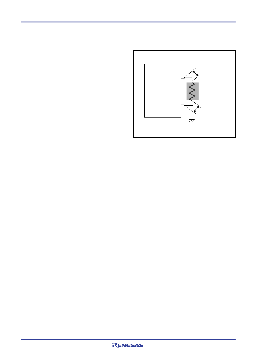
Connect the CNVSS/(VPP) pin the shortest possible to the GND
pattern which is supplied to the VSS pin of the microcomputer.
In addition connecting an approximately 5 k
resistor in series to
the GND could improve noise immunity. In this case as well as the
above mention, connect the pin the shortest possible to the GND
pattern which is supplied to the VSS pin of the microcomputer.
Reason
The CNVSS/(VPP) pin is the power source input pin for the built-in
QzROM. When programming in the QzROM, the impedance of the
VPP pin is low to allow the electric current for writing to flow into
the built-in QzROM. Because of this, noise can enter easily.If
noise enters the CNVSS/(VPP) pin, abnormal instruction codes or
data are read from the QzROM, which may cause a program run-
away.
NOTES ON QzROM
Notes On QzROM Writing Orders
When ordering the QzROM product shipped after writing, submit
the mask file (extension : .msk) which is made by the mask file
converter MM.
Be sure to set the ROM option (“MASK option“ written in the mask
file converter) setup when making the mask file by using the mask
file converter MM.
Notes On ROM Code Protect
(QzROM product shipped after writing)
As for the QzROM product shipped after writing, the ROM code
protect is specified according to the ROM option setup data in the
mask file which is submitted at ordering. The ROM option setup
data in the mask file is “0016” for protect enabled or “FF16” for pro-
tect disabled. Therefore, the contents of the ROM code protect
address (other than the user ROM area)of the QzROM product
shipped after writing is “0016” or “FF16”.
Note that the mask file which has nothing at the ROM option data
or has the data other than “0016” and “FF16” can not be accepted.
DATA REQUIRED FOR QzROM WRITING
ORDERS
The following are necessary when ordering a QzROM product
shipped after writing:
1.QzROM Writing Confirmation Form*
2.Mark Specification Form*
3.ROM data...........Mask file
*For the QzROM writing confirmation form and the mark specifica-
tion form, refer to the “Renesas Technology Corp.” Homepage
(http://www.renesas.com/homepage.jsp).
Note that we cannot deal with special font marking (customer's
trademark etc.) in QzROM microcomputer.
Fig. 46 Wiring for the CNVSS/(VPP) pin
CNVSS/(VPP)
VSS
The shortest
Approx. 5k
(Note)
Note. Shows the microcomputer's pin.
相關(guān)PDF資料 |
PDF描述 |
|---|---|
| M38869MFAHP | 8-BIT, FLASH, 10 MHz, MICROCONTROLLER, PQFP80 |
| M38B57MC-XXXFP | 8-BIT, MROM, 4.19 MHz, MICROCONTROLLER, PQFP80 |
| M38B79FFFP | 8-BIT, FLASH, 4.2 MHz, MICROCONTROLLER, PQFP100 |
| M38B79MFH-XXXXFP | 8-BIT, MROM, 4.2 MHz, MICROCONTROLLER, PQFP100 |
| M38C13M6-XXXFP | 8-BIT, MROM, 4 MHz, MICROCONTROLLER, PQFP64 |
相關(guān)代理商/技術(shù)參數(shù) |
參數(shù)描述 |
|---|---|
| M38827G6-XXXHP | 制造商:RENESAS 制造商全稱(chēng):Renesas Technology Corp 功能描述:SINGLE-CHIP 8-BIT CMOS MICROCOMPUTER |
| M38827G7-XXXHP | 制造商:RENESAS 制造商全稱(chēng):Renesas Technology Corp 功能描述:SINGLE-CHIP 8-BIT CMOS MICROCOMPUTER |
| M38827G8-XXXHP | 制造商:RENESAS 制造商全稱(chēng):Renesas Technology Corp 功能描述:SINGLE-CHIP 8-BIT CMOS MICROCOMPUTER |
| M38827G9-XXXHP | 制造商:RENESAS 制造商全稱(chēng):Renesas Technology Corp 功能描述:SINGLE-CHIP 8-BIT CMOS MICROCOMPUTER |
| M38827GA-XXXHP | 制造商:RENESAS 制造商全稱(chēng):Renesas Technology Corp 功能描述:SINGLE-CHIP 8-BIT CMOS MICROCOMPUTER |
發(fā)布緊急采購(gòu),3分鐘左右您將得到回復(fù)。