- 您現(xiàn)在的位置:買賣IC網(wǎng) > PDF目錄45046 > M38507F8FP 8-BIT, MROM, 8 MHz, MICROCONTROLLER, PDSO42 PDF資料下載
參數(shù)資料
| 型號(hào): | M38507F8FP |
| 元件分類: | 微控制器/微處理器 |
| 英文描述: | 8-BIT, MROM, 8 MHz, MICROCONTROLLER, PDSO42 |
| 封裝: | 0.450 INCH, 0.80 MM PITCH, PLASTIC, SSOP-42 |
| 文件頁數(shù): | 131/287頁 |
| 文件大小: | 2969K |
| 代理商: | M38507F8FP |
第1頁第2頁第3頁第4頁第5頁第6頁第7頁第8頁第9頁第10頁第11頁第12頁第13頁第14頁第15頁第16頁第17頁第18頁第19頁第20頁第21頁第22頁第23頁第24頁第25頁第26頁第27頁第28頁第29頁第30頁第31頁第32頁第33頁第34頁第35頁第36頁第37頁第38頁第39頁第40頁第41頁第42頁第43頁第44頁第45頁第46頁第47頁第48頁第49頁第50頁第51頁第52頁第53頁第54頁第55頁第56頁第57頁第58頁第59頁第60頁第61頁第62頁第63頁第64頁第65頁第66頁第67頁第68頁第69頁第70頁第71頁第72頁第73頁第74頁第75頁第76頁第77頁第78頁第79頁第80頁第81頁第82頁第83頁第84頁第85頁第86頁第87頁第88頁第89頁第90頁第91頁第92頁第93頁第94頁第95頁第96頁第97頁第98頁第99頁第100頁第101頁第102頁第103頁第104頁第105頁第106頁第107頁第108頁第109頁第110頁第111頁第112頁第113頁第114頁第115頁第116頁第117頁第118頁第119頁第120頁第121頁第122頁第123頁第124頁第125頁第126頁第127頁第128頁第129頁第130頁當(dāng)前第131頁第132頁第133頁第134頁第135頁第136頁第137頁第138頁第139頁第140頁第141頁第142頁第143頁第144頁第145頁第146頁第147頁第148頁第149頁第150頁第151頁第152頁第153頁第154頁第155頁第156頁第157頁第158頁第159頁第160頁第161頁第162頁第163頁第164頁第165頁第166頁第167頁第168頁第169頁第170頁第171頁第172頁第173頁第174頁第175頁第176頁第177頁第178頁第179頁第180頁第181頁第182頁第183頁第184頁第185頁第186頁第187頁第188頁第189頁第190頁第191頁第192頁第193頁第194頁第195頁第196頁第197頁第198頁第199頁第200頁第201頁第202頁第203頁第204頁第205頁第206頁第207頁第208頁第209頁第210頁第211頁第212頁第213頁第214頁第215頁第216頁第217頁第218頁第219頁第220頁第221頁第222頁第223頁第224頁第225頁第226頁第227頁第228頁第229頁第230頁第231頁第232頁第233頁第234頁第235頁第236頁第237頁第238頁第239頁第240頁第241頁第242頁第243頁第244頁第245頁第246頁第247頁第248頁第249頁第250頁第251頁第252頁第253頁第254頁第255頁第256頁第257頁第258頁第259頁第260頁第261頁第262頁第263頁第264頁第265頁第266頁第267頁第268頁第269頁第270頁第271頁第272頁第273頁第274頁第275頁第276頁第277頁第278頁第279頁第280頁第281頁第282頁第283頁第284頁第285頁第286頁第287頁
3850 Group (Spec. H) User’s Manual
APPENDIX
3.1 Electrical characteristics
3-8
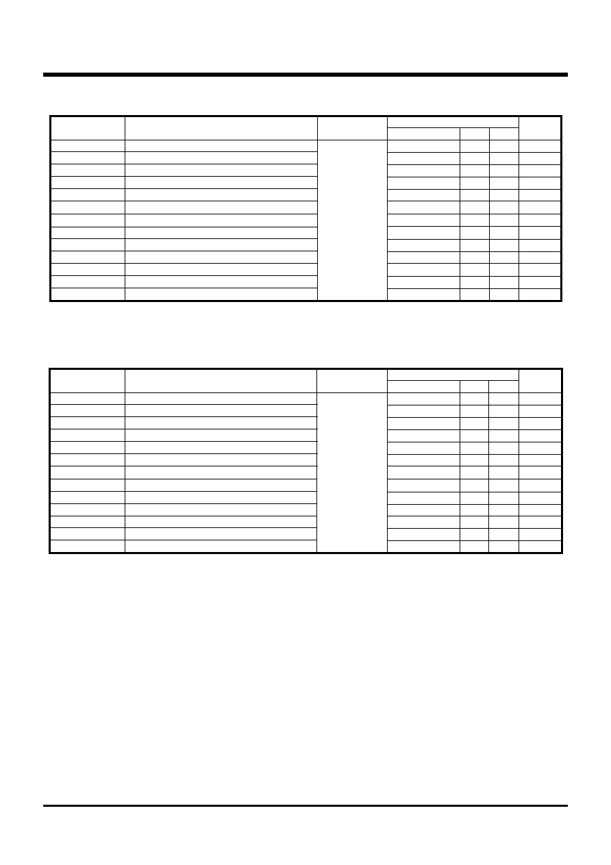
Table 3.1.9 Switching characteristics (1)
(VCC = 4.0 to 5.5 V, VSS = 0 V, Ta = –20 to 85 °C, unless otherwise noted)
Table 3.1.10 Switching characteristics (2)
(VCC = 2.7 to 5.5 V, VSS = 0 V, Ta = –20 to 85 °C, unless otherwise noted)
Serial I/O1 clock output “H” pulse width
Serial I/O1 clock output “L” pulse width
Serial I/O1 output delay time (Note 1)
Serial I/O1 output valid time (Note 1)
Serial I/O1 clock output rising time
Serial I/O1 clock output falling time
Serial I/O2 clock output “H” pulse width
Serial I/O2 clock output “L” pulse width
Serial I/O2 output delay time (Note 2)
Serial I/O2 output valid time (Note 2)
Serial I/O2 clock output falling time
CMOS output rising time (Note 3)
CMOS output falling time (Note 3)
tWH (SCLK1)
tWL (SCLK1)
td (SCLK1-TXD)
tv (SCLK1-TXD)
tr (SCLK1)
tf (SCLK1)
tWH (SCLK2)
tWL (SCLK2)
td (SCLK2-SOUT2)
tv (SCLK2-SOUT2)
tf (SCLK2)
tr (CMOS)
tf (CMOS)
Limits
ns
Parameter
Min.
tC(SCLK1)/2–30
–30
tC(SCLK2)/2–160
0
Typ.
10
Max.
140
30
200
30
Symbol
Unit
Notes 1: When the P25/TXD P-channel output disable bit of the UART control register (bit 4 of address 001B16) is “0”.
2: When the P01/SOUT2 and P02/SCLK2 P-channel output disable bit of the Serial I/O2 control register 1 (bit 7 of address 001516) is “0”.
3: The XOUT pin is excluded.
Test conditions
Fig.3.1.1
Serial I/O1 clock output “H” pulse width
Serial I/O1 clock output “L” pulse width
Serial I/O1 output delay time (Note 1)
Serial I/O1 output valid time (Note 1)
Serial I/O1 clock output rising time
Serial I/O1 clock output falling time
Serial I/O2 clock output “H” pulse width
Serial I/O2 clock output “L” pulse width
Serial I/O2 output delay time (Note 2)
Serial I/O2 output valid time (Note 2)
Serial I/O2 clock output falling time
CMOS output rising time (Note 3)
CMOS output falling time (Note 3)
tWH (SCLK1)
tWL (SCLK1)
td (SCLK1-TXD)
tv (SCLK1-TXD)
tr (SCLK1)
tf (SCLK1)
tWH (SCLK2)
tWL (SCLK2)
td (SCLK2-SOUT2)
tv (SCLK2-SOUT2)
tf (SCLK2)
tr (CMOS)
tf (CMOS)
Limits
ns
Parameter
Min.
tC(SCLK1)/2–50
–30
tC(SCLK2)/2–240
0
Typ.
20
Max.
350
50
400
50
Symbol
Unit
Notes 1: When the P25/TXD P-channel output disable bit of the UART control register (bit 4 of address 001B16) is “0”.
2: When the P01/SOUT2 and P02/SCLK2 P-channel output disable bit of the Serial I/O2 control register 1 (bit 7 of address 001516) is “0”.
3: The XOUT pin is excluded.
Test conditions
Fig.3.1.1
相關(guān)PDF資料 |
PDF描述 |
|---|---|
| M38504E6FP | 8-BIT, MROM, 8 MHz, MICROCONTROLLER, PDSO42 |
| M38504E6SP | 8-BIT, MROM, 8 MHz, MICROCONTROLLER, PDIP42 |
| M38504M6-XXXSP | 8-BIT, MROM, 8 MHz, MICROCONTROLLER, PDIP42 |
| M38504M6-XXXFP | 8-BIT, MROM, 8 MHz, MICROCONTROLLER, PDSO42 |
| M38503M4H-XXXFP | 8-BIT, MROM, 8 MHz, MICROCONTROLLER, PDSO42 |
相關(guān)代理商/技術(shù)參數(shù) |
參數(shù)描述 |
|---|---|
| M38507F8FP#U1 | 制造商:Renesas Electronics Corporation 功能描述:MCU 8BIT 740 CISC 32KB FLASH 5V 42SSOP - Trays |
| M38507F8FP#W1 | 制造商:Renesas Electronics Corporation 功能描述:FLASH 8-BIT 2.7 TO 5.5V PBFREE |
| M38507F8FP(#U1) | 制造商:Renesas Electronics Corporation 功能描述: |
| M3851 BK001 | 制造商:Alpha Wire Company 功能描述:CBL 7COND 14AWG BLK 1000' |
| M3851 BK002 | 制造商:Alpha Wire Company 功能描述:CBL 7COND 14AWG BLK 500' |
發(fā)布緊急采購,3分鐘左右您將得到回復(fù)。