- 您現(xiàn)在的位置:買賣IC網(wǎng) > PDF目錄69013 > M37549G1FP 8-BIT, MROM, 8 MHz, MICROCONTROLLER, PDSO24 PDF資料下載
參數(shù)資料
| 型號: | M37549G1FP |
| 元件分類: | 微控制器/微處理器 |
| 英文描述: | 8-BIT, MROM, 8 MHz, MICROCONTROLLER, PDSO24 |
| 封裝: | 5.30 X 10.10 MM, 0.80 MM PITCH, PLASTIC, SSOP-24 |
| 文件頁數(shù): | 19/86頁 |
| 文件大小: | 1375K |
| 代理商: | M37549G1FP |
第1頁第2頁第3頁第4頁第5頁第6頁第7頁第8頁第9頁第10頁第11頁第12頁第13頁第14頁第15頁第16頁第17頁第18頁當前第19頁第20頁第21頁第22頁第23頁第24頁第25頁第26頁第27頁第28頁第29頁第30頁第31頁第32頁第33頁第34頁第35頁第36頁第37頁第38頁第39頁第40頁第41頁第42頁第43頁第44頁第45頁第46頁第47頁第48頁第49頁第50頁第51頁第52頁第53頁第54頁第55頁第56頁第57頁第58頁第59頁第60頁第61頁第62頁第63頁第64頁第65頁第66頁第67頁第68頁第69頁第70頁第71頁第72頁第73頁第74頁第75頁第76頁第77頁第78頁第79頁第80頁第81頁第82頁第83頁第84頁第85頁第86頁
Rev.2.02
Mar 31, 2009
Page 24 of 81
REJ03B0202-0202
7549 Group
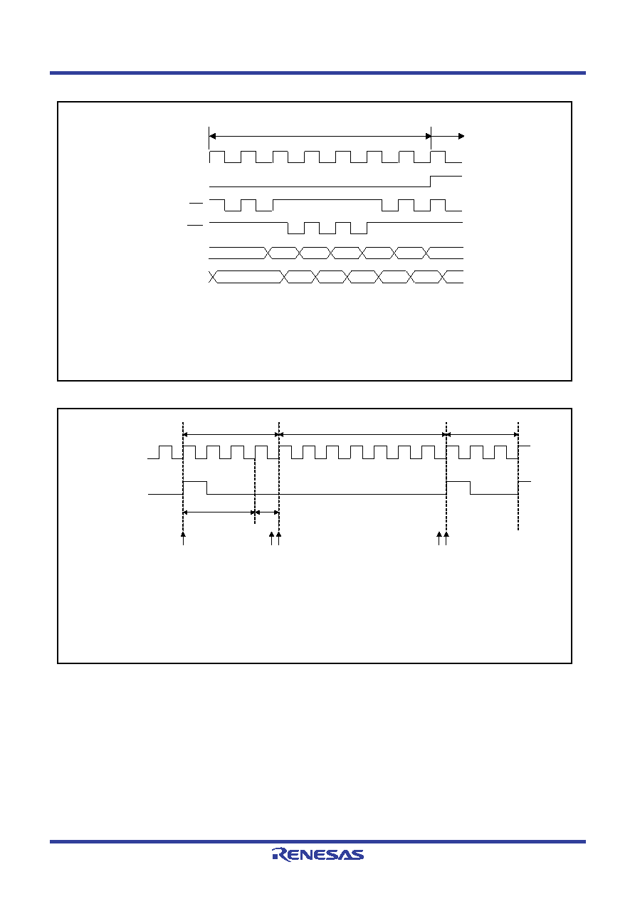
Fig 21. Interrupt sequence
Fig 22. Timing of interrupt request generation, interrupt request bit, and interrupt acceptance
<Notes>
The interrupt request bit may be set to “1” in the following cases.
<When switching external interrupt active edge>
INT0 interrupt edge selection bit
(bit 0 of Interrupt edge selection register (address 003A16))
INT1 interrupt edge selection bit
(bit 1 of Interrupt edge selection register)
If it is not necessary to generate an interrupt synchronized with
these settings, take the following sequence.
(1)Set the corresponding enable bit to “0” (disabled).
(2)Set the interrupt edge selection bit (the active edge switch
bit) or the interrupt source bit.
(3)Set the corresponding interrupt request bit to “0” after one
or more instructions have been executed.
(4)Set the corresponding interrupt enable bit to “1” (enabled).
φ
SYNC
RD
WR
Push onto stack
Vector fetch
Address bus
Data bus
Execute interrupt
routine
PC
S,SPS
S-1,SPS S-2,SPS
BL
BH
AL,AH
Not used
PCH
PCL
PS
AL
AH
SYNC : CPU operation code fetch cycle
(This is an internal signal that cannot be observed from the external unit.)
BL, BH: Vector address of each interrupt
AL, AH: Jump destination address of each interrupt
SPS
: “0016” or “0116”
([SPS] is a page selected by the stack page selection bit of CPU mode register.)
T1
(1) The interrupt request bit for an interrupt request generated during period 1 is set to “1” at timing point IR1.
(2) The interrupt request bit for an interrupt request generated during period 2 is set to “1” at timing point IR1 or IR2.
The timing point at which the bit is set to “1” varies depending on conditions. When two or more interrupt
requests are generated during the period 2, each request bit may be set to “1” at timing point IR1 or IR2
separately.
T1 T2 T3 : Interrupt acceptance timing points
IR1 IR2 : Timings points at which the interrupt request bit is set to “1”.
Note : Period 2 indicates the last
φ cycle during one instruction cycle.
IR1 T2
SYNC
IR2 T3
12
Internal clock
φ
Instruction cycle
Push onto stack
Vector fetch
Instruction cycle
相關(guān)PDF資料 |
PDF描述 |
|---|---|
| M37560M8-XXXFP | 8-BIT, MROM, 8 MHz, MICROCONTROLLER, PQFP100 |
| M37560EFDFP | 8-BIT, OTPROM, 8 MHz, MICROCONTROLLER, PQFP100 |
| M37560MFD-XXXFP | 8-BIT, MROM, 8 MHz, MICROCONTROLLER, PQFP100 |
| M37560EFFP | 8-BIT, OTPROM, 8 MHz, MICROCONTROLLER, PQFP100 |
| M37560M8-XXXGP | 8-BIT, MROM, 8 MHz, MICROCONTROLLER, PQFP100 |
相關(guān)代理商/技術(shù)參數(shù) |
參數(shù)描述 |
|---|---|
| M37549G1-XXXFP | 制造商:RENESAS 制造商全稱:Renesas Technology Corp 功能描述:SINGLE-CHIP 8-BIT CMOS MICROCOMPUTER |
| M37549G2FP | 制造商:RENESAS 制造商全稱:Renesas Technology Corp 功能描述:SINGLE-CHIP 8-BIT CMOS MICROCOMPUTER |
| M37549G2-XXXFP | 制造商:RENESAS 制造商全稱:Renesas Technology Corp 功能描述:SINGLE-CHIP 8-BIT CMOS MICROCOMPUTER |
| M37549G3FP | 制造商:RENESAS 制造商全稱:Renesas Technology Corp 功能描述:SINGLE-CHIP 8-BIT CMOS MICROCOMPUTER |
| M37549G3-XXXFP | 制造商:RENESAS 制造商全稱:Renesas Technology Corp 功能描述:SINGLE-CHIP 8-BIT CMOS MICROCOMPUTER |
發(fā)布緊急采購,3分鐘左右您將得到回復(fù)。