- 您現(xiàn)在的位置:買賣IC網(wǎng) > PDF目錄69010 > M34506M4-XXXFP 4-BIT, MROM, MICROCONTROLLER, PDSO20 PDF資料下載
參數(shù)資料
| 型號: | M34506M4-XXXFP |
| 元件分類: | 微控制器/微處理器 |
| 英文描述: | 4-BIT, MROM, MICROCONTROLLER, PDSO20 |
| 封裝: | 5.30 X 12.60 MM, 1.27 MM PITCH, PLASTIC, SOP-20 |
| 文件頁數(shù): | 91/114頁 |
| 文件大?。?/td> | 937K |
| 代理商: | M34506M4-XXXFP |
第1頁第2頁第3頁第4頁第5頁第6頁第7頁第8頁第9頁第10頁第11頁第12頁第13頁第14頁第15頁第16頁第17頁第18頁第19頁第20頁第21頁第22頁第23頁第24頁第25頁第26頁第27頁第28頁第29頁第30頁第31頁第32頁第33頁第34頁第35頁第36頁第37頁第38頁第39頁第40頁第41頁第42頁第43頁第44頁第45頁第46頁第47頁第48頁第49頁第50頁第51頁第52頁第53頁第54頁第55頁第56頁第57頁第58頁第59頁第60頁第61頁第62頁第63頁第64頁第65頁第66頁第67頁第68頁第69頁第70頁第71頁第72頁第73頁第74頁第75頁第76頁第77頁第78頁第79頁第80頁第81頁第82頁第83頁第84頁第85頁第86頁第87頁第88頁第89頁第90頁當(dāng)前第91頁第92頁第93頁第94頁第95頁第96頁第97頁第98頁第99頁第100頁第101頁第102頁第103頁第104頁第105頁第106頁第107頁第108頁第109頁第110頁第111頁第112頁第113頁第114頁
Rev.2.00
Aug 28, 2006
page 76 of 119
7643 Group
REJ03B0054-0200
Notes 1: Test conditions: IOHL =
± 5mA, CL = 50 pF
2: twL(RD) = ((n + 0.5) tc(PHI)) – 5 ns (n = wait number)
twL(WR) = ((n + 0.5) tc(PHI)) – 5 ns (n = wait number)
For example, two software waits, PHI = 12 MHz operating
twL(RD) = 2.5 tc(PHI) – 5 ns = 203.33 ns
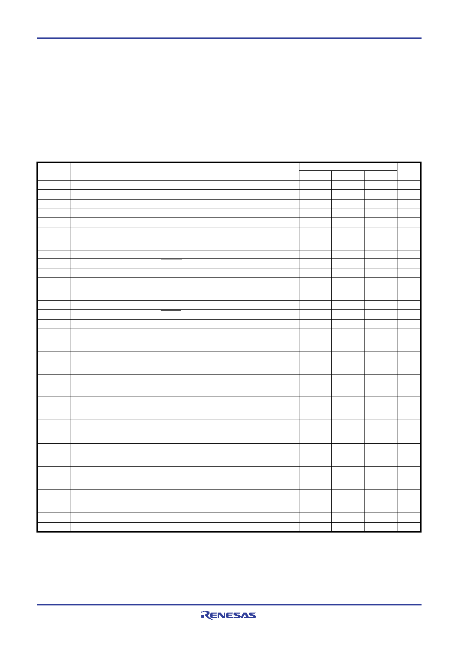
Table 15 Recommended operating conditions (Vcc = 3.0 to 3.6 V, Vss = 0 V, Ta = –20 to 70°C, unless otherwise noted)
Power source voltage
Analog reference voltage
Power source voltage
Analog reference voltage
DC-DC converter voltage
“H” input voltage
P00–P07, P10–P17, P20–P27,
P30–P37, P40–P44, P50–P57,
P60–P67, P70–P74, P80–P87
“H” input voltage (Selecting VIHL level input) P20–P27
“H” input voltage
RESET, XIN, XCIN, CNVss
“H” input voltage
USB D+, USB D–
“L” input voltage
P00–P07, P10–P17, P20–P27,
P30–P37, P40–P44, P50–P57,
P60–P67, P70–P74, P80–P87
“L” input voltage (Selecting VIHL level input)
P20–P27
“L” input voltage
RESET, XIN, XCIN, CNVss
“L” input voltage
USB D+, USB D–
“H” total peak output current
P00–P07, P10–P17, P20–P27,
(Note 1)P30–P37, P40–P44, P50–P57,
P60–P67, P70–P74, P80–P87
“L” total peak output current
P00–P07, P10–P17, P20–P27,
(Note 1)P30–P37, P40–P44, P50–P57,
P60–P67, P70–P74, P80–P87
“H” total average output current P00–P07, P10–P17, P20–P27,
(Note 1)P30–P37, P40–P44, P50–P57,
P60–P67, P70–P74, P80–P87
“L” total average output current P00–P07, P10–P17, P20–P27,
(Note 1)P30–P37, P40–P44, P50–P57,
P60–P67, P70–P74, P80–P87
“H” peak output current
P00–P07, P10–P17, P20–P27,
(Note 2)P30–P37, P40–P44, P50–P57,
P60–P67, P70–P74, P80–P87
“L” peak output current
P00–P07, P10–P17, P20–P27,
(Note 2)P30–P37, P40–P44, P50–P57,
P60–P67, P70–P74, P80–P87
“H” average output current
P00–P07, P10–P17, P20–P27,
(Note 3)P30–P37, P40–P44, P50–P57,
P60–P67, P70–P74, P80–P87
“L” average output current
P00–P07, P10–P17, P20–P27,
(Note 3)P30–P37, P40–P44, P50–P57,
P60–P67, P70–P74, P80–P87
Main clock input frequency (Notes 4, 5)
Sub-clock input frequency (Notes 4, 6)
VCC
AVcc
VSS
AVSS
Ext. Cap.
VIH
VIL
ΣIOH(peak)
ΣIOL(peak)
ΣIOH(avg)
ΣIOL(avg)
IOH(peak)
IOL(peak)
IOH(avg)
IOL(avg)
f(XIN)
f(XCIN)
Limits
V
Parameter
Min.
3.0
0.8VCC
0.5VCC
0.8VCC
2.0
0
Typ.
3.3
0
3.3
Max.
3.6
VCC
Symbol
Unit
3.6
VCC
Recommended Operating Conditions
In Vcc = 3 V
0
1
VCC
0.2VCC
0.16VCC
0.2VCC
0.8
–80
80
–40
40
–10
10
–5.0
V
mA
32.768
5.0
24
50/5.0
MHz
kHz/MHz
Notes 1: The total peak output current is the peak value of the peak currents flowing through all the applicable ports. The total average output current is the average
value measured over 100 ms flowing through all the applicable ports.
2: The peak output current is the peak current flowing in each port.
3: The average output current is an average value measured over 100 ms.
4: The duty of oscillation frequency is 50
%.
5: Connect a ceramic resonator or a quartz-crystal oscillator between the XIN and XOUT pins. Its maximum oscillation frequency must be 24 MHz. However,
make sure to set
φ to 6 MHz or slower. More faster clocks are required as the f(XIN) when using the frequency synthesizer as possible.
6: Connect a ceramic resonator or a quartz-crystal oscillator between the XCIN and XCOUT pins. Its maximum oscillation frequency must be 50 kHz. Input an
external clock having 5 MHz (max.) frequency from the XCIN pin.
相關(guān)PDF資料 |
PDF描述 |
|---|---|
| M34506E4FP | 4-BIT, OTPROM, MICROCONTROLLER, PDSO20 |
| M34508G4HFP | 4-BIT, MROM, 6 MHz, MICROCONTROLLER, PDSO20 |
| M34508G4GP | 4-BIT, MROM, 6 MHz, MICROCONTROLLER, PDSO20 |
| M34508G4H-XXXFP | 4-BIT, MROM, 6 MHz, MICROCONTROLLER, PDSO20 |
| M34508G4-XXXFP | 4-BIT, MROM, 6 MHz, MICROCONTROLLER, PDSO20 |
相關(guān)代理商/技術(shù)參數(shù) |
參數(shù)描述 |
|---|---|
| M34507E4FP | 制造商:RENESAS 制造商全稱:Renesas Technology Corp 功能描述:SINGLE-CHIP 4-BIT CMOS MICROCOMPUTER |
| M34507M2-XXXFP | 制造商:RENESAS 制造商全稱:Renesas Technology Corp 功能描述:4-BIT CISC SINGLE-CHIP MICROCOMPUTER 4500 SERIES |
| M34507M4-XXXFP | 制造商:RENESAS 制造商全稱:Renesas Technology Corp 功能描述:SINGLE-CHIP 4-BIT CMOS MICROCOMPUTER |
| M34508G4FP | 制造商:RENESAS 制造商全稱:Renesas Technology Corp 功能描述:SINGLE-CHIP 4-BIT CMOS MICROCOMPUTER |
| M34508G4GP | 制造商:RENESAS 制造商全稱:Renesas Technology Corp 功能描述:SINGLE-CHIP 4-BIT CMOS MICROCOMPUTER |
發(fā)布緊急采購,3分鐘左右您將得到回復(fù)。