- 您現(xiàn)在的位置:買賣IC網(wǎng) > PDF目錄69010 > M34501E4FP 4-BIT, OTPROM, 4.4 MHz, MICROCONTROLLER, PDSO20 PDF資料下載
參數(shù)資料
| 型號: | M34501E4FP |
| 元件分類: | 微控制器/微處理器 |
| 英文描述: | 4-BIT, OTPROM, 4.4 MHz, MICROCONTROLLER, PDSO20 |
| 封裝: | 0.300 INCH, PLASTIC, SOP-20 |
| 文件頁數(shù): | 156/213頁 |
| 文件大?。?/td> | 3014K |
| 代理商: | M34501E4FP |
第1頁第2頁第3頁第4頁第5頁第6頁第7頁第8頁第9頁第10頁第11頁第12頁第13頁第14頁第15頁第16頁第17頁第18頁第19頁第20頁第21頁第22頁第23頁第24頁第25頁第26頁第27頁第28頁第29頁第30頁第31頁第32頁第33頁第34頁第35頁第36頁第37頁第38頁第39頁第40頁第41頁第42頁第43頁第44頁第45頁第46頁第47頁第48頁第49頁第50頁第51頁第52頁第53頁第54頁第55頁第56頁第57頁第58頁第59頁第60頁第61頁第62頁第63頁第64頁第65頁第66頁第67頁第68頁第69頁第70頁第71頁第72頁第73頁第74頁第75頁第76頁第77頁第78頁第79頁第80頁第81頁第82頁第83頁第84頁第85頁第86頁第87頁第88頁第89頁第90頁第91頁第92頁第93頁第94頁第95頁第96頁第97頁第98頁第99頁第100頁第101頁第102頁第103頁第104頁第105頁第106頁第107頁第108頁第109頁第110頁第111頁第112頁第113頁第114頁第115頁第116頁第117頁第118頁第119頁第120頁第121頁第122頁第123頁第124頁第125頁第126頁第127頁第128頁第129頁第130頁第131頁第132頁第133頁第134頁第135頁第136頁第137頁第138頁第139頁第140頁第141頁第142頁第143頁第144頁第145頁第146頁第147頁第148頁第149頁第150頁第151頁第152頁第153頁第154頁第155頁當前第156頁第157頁第158頁第159頁第160頁第161頁第162頁第163頁第164頁第165頁第166頁第167頁第168頁第169頁第170頁第171頁第172頁第173頁第174頁第175頁第176頁第177頁第178頁第179頁第180頁第181頁第182頁第183頁第184頁第185頁第186頁第187頁第188頁第189頁第190頁第191頁第192頁第193頁第194頁第195頁第196頁第197頁第198頁第199頁第200頁第201頁第202頁第203頁第204頁第205頁第206頁第207頁第208頁第209頁第210頁第211頁第212頁第213頁
1-34
HARDWARE
4501 Group User’s Manual
FUNCTION BLOCK OPERATIONS
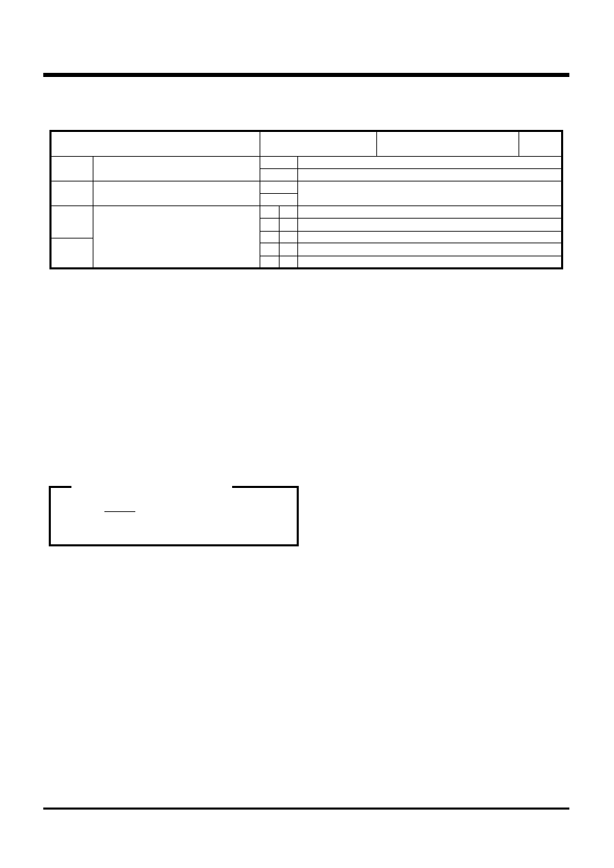
Q13
Q12
A-D control register Q1
A-D operation mode selection bit
Not used
Analog input pin selection bits
at reset : 00002
at RAM back-up : state retained
0
1
0
1
Q11
0
1
A-D conversion mode
Comparator mode
This bit has no function, but read/write is enabled.
Selected pins
AIN0
AIN1
Not available
Note: “R” represents read enabled, and “W” represents write enabled.
Q10
0
1
0
1
(1) Operating at A-D conversion mode
The A-D conversion mode is set by setting the bit 3 of register Q1 to “0.”
(2) Successive comparison register AD
Register AD stores the A-D conversion result of an analog input in
10-bit digital data format. The contents of the high-order 8 bits of
this register can be stored in register B and register A with the
TABAD instruction. The contents of the low-order 2 bits of this reg-
ister can be stored into the high-order 2 bits of register A with the
TALA instruction. However, do not execute these instructions dur-
ing A-D conversion.
When the contents of register AD is n, the logic value of the com-
parison voltage Vref generated from the built-in DA converter can
be obtained with the reference voltage VDD by the following for-
mula:
Logic value of comparison voltage Vref
Vref =
n
n: The value of register AD (n = 0 to 1023)
VDD
1024
R/W
Table 12 A-D control registers
(3) A-D conversion completion flag (ADF)
A-D conversion completion flag (ADF) is set to “1” when A-D con-
version completes. The state of ADF flag can be examined with the
skip instruction (SNZAD). Use the interrupt control register V2 to
select the interrupt or the skip instruction.
The ADF flag is cleared to “0” when the interrupt occurs or when
the next instruction is skipped with the skip instruction.
(4) A-D conversion start instruction (ADST)
A-D conversion starts when the ADST instruction is executed. The
conversion result is automatically stored in the register AD.
(5) A-D control register Q1
Register Q1 is used to select the operation mode and one of ana-
log input pins.
Q11
Q10
(6) Operation description
A-D conversion is started with the A-D conversion start instruction
(ADST). The internal operation during A-D conversion is as follows:
When the A-D conversion starts, the register AD is cleared to
“00016.”
Next, the topmost bit of the register AD is set to “1,” and the
comparison voltage Vref is compared with the analog input volt-
age VIN.
When the comparison result is Vref < VIN, the topmost bit of the
register AD remains set to “1.” When the comparison result is
Vref > VIN, it is cleared to “0.”
The 4501 Group repeats this operation to the lowermost bit of the
register AD to convert an analog value to a digital value. A-D con-
version stops after 62 machine cycles (46.5
s when f(XIN) = 4.0
MHz in high-speed mode) from the start, and the conversion result
is stored in the register AD. An A-D interrupt activated condition is
satisfied and the ADF flag is set to “1” as soon as A-D conversion
completes (Figure 28).
相關(guān)PDF資料 |
PDF描述 |
|---|---|
| M34501M2-XXXFP | 4-BIT, MROM, MICROCONTROLLER, PDSO20 |
| M34501E4FP | 4-BIT, OTPROM, MICROCONTROLLER, PDSO20 |
| M34501M4-XXXFP | 4-BIT, MROM, MICROCONTROLLER, PDSO20 |
| M34501E4FP | 4-BIT, OTPROM, MICROCONTROLLER, PDSO20 |
| M34502M2-XXXFP | 4-BIT, MROM, MICROCONTROLLER, PDSO24 |
相關(guān)代理商/技術(shù)參數(shù) |
參數(shù)描述 |
|---|---|
| M34501M2 | 制造商:MITSUBISHI 制造商全稱:Mitsubishi Electric Semiconductor 功能描述:SINGLE-CHIP 4-BIT CMOS MICROCOMPUTER |
| M34501M2-XXXFP | 制造商:RENESAS 制造商全稱:Renesas Technology Corp 功能描述:SINGLE-CHIP 4-BIT CMOS MICROCOMPUTER |
| M34501M4 | 制造商:MITSUBISHI 制造商全稱:Mitsubishi Electric Semiconductor 功能描述:SINGLE-CHIP 4-BIT CMOS MICROCOMPUTER |
| M34501M4-XXXFP | 制造商:MITSUBISHI 制造商全稱:Mitsubishi Electric Semiconductor 功能描述:SINGLE-CHIP 4-BIT CMOS MICROCOMPUTER |
| M34502E4 | 制造商:RENESAS 制造商全稱:Renesas Technology Corp 功能描述:SINGLE-CHIP 4-BIT CMOS MICROCOMPUTER |
發(fā)布緊急采購,3分鐘左右您將得到回復。