- 您現(xiàn)在的位置:買賣IC網(wǎng) > PDF目錄98005 > M32176F2TFP 32-BIT, FLASH, 40 MHz, RISC MICROCONTROLLER, PQFP144 PDF資料下載
參數(shù)資料
| 型號: | M32176F2TFP |
| 元件分類: | 微控制器/微處理器 |
| 英文描述: | 32-BIT, FLASH, 40 MHz, RISC MICROCONTROLLER, PQFP144 |
| 封裝: | 20 X 20 MM, 0.50 MM PITCH, PLASTIC, LQFP-144 |
| 文件頁數(shù): | 8/36頁 |
| 文件大?。?/td> | 342K |
| 代理商: | M32176F2TFP |
第1頁第2頁第3頁第4頁第5頁第6頁第7頁當前第8頁第9頁第10頁第11頁第12頁第13頁第14頁第15頁第16頁第17頁第18頁第19頁第20頁第21頁第22頁第23頁第24頁第25頁第26頁第27頁第28頁第29頁第30頁第31頁第32頁第33頁第34頁第35頁第36頁
16
32176 Group
Mitsubishi Microcomputers
SINGLE-CHIP 32-BIT CMOS MICROCOMPUTER
Under Development
Jan. 30, 2003
Rev.1.4
Built-in flash memory and RAM
The M32176F4VFP/M32176F4TFP contains 512K bytes
flash memory and 24K bytes RAM, the M32176F3VFP/
M32176F3TFP contains 384K bytes flash memory and 24K
bytes RAM, the M32176F2VFP/ M32176F2TFP contains
256K bytes flash memory and 24K bytes RAM.
The internal flash memory can be programmed while being
mounted on the printed circuit board (on-board program-
ming). Use of flash memory allows the same chip as those
used in mass production to be used beginning with the de-
velopment stage. This means that system development can
be proceeded without having to change the printed circuit
boards during the entire course, from prototype to mass pro-
duction.
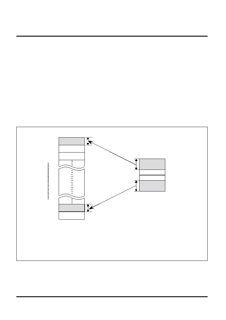
Built-in Virtual-Flash Emulation Function
Internal flash memory, which is divided from the first address in
units of 8K bytes (L banks), can be replaced in 8K bytes blocks
(H’0080 4000-H’0080 5FFF, H’0080 8000-H’0080 9FFF) from
the beginning of the internal RAM. And also the internal flash
memory, which is divided from the first address in units of 4K
bytes area (All S banks), can be replaced within two 4K bytes
areas (H’0080 6000-H’0080 7FFF).
This function allows parts of the program which are fre-
quently changed during development to be altered or evalu-
ated without having to reset the microcomputer each time.
What’s more, when combined with the realtime debugger,
this function helps to reduce the program evaluation period,
because data in the RAM can be rewritten without requiring
any CPU load.
H'0000 0000
H'0000 2000
< Internal flash >
H'0080 4000
H'0080 5FFF
L bank 0
(8K bytes)
H'0000 4000
8K bytes
H'0000 1FFF
H'0000 3FFF
H'0000 5FFF
H'0007 E000
H'0007 FFFF
H'0007 C000
H'0007 DFFF
4K bytes
H'0080 6000
H'0080 7FFF
8K bytes
H'0080 8000
H'0080 9FFF
L bank 1
(8K bytes)
L bank 2
(8K bytes)
L bank 62
(8K bytes)
L bank 63
(8K bytes)
< Internal RAM >
Figure 8. Virtual-Flash Emulation Areas of the M32176F4VFP/M32176F4TFP (Replaced in Units of 8K bytes)
Notes: If the same bank area is set in multiple virtual-flash bank registers and the virtual-flash emulation enable bit is enabled, the
corresponding internal RAM area is assigned to either bank register according to the priority FELBANK0 > FESBANK0 >
FESBANK1 > FELBANK1.
When access is made to the 8K bytes area (L bank) specified with virtual-flash bank register 0, the internal RAM area is
accessed. During virtual-flash emulation mode, RAM data can read and written to and from both the internal RAM area and
the virtual-flash setup area.
相關PDF資料 |
PDF描述 |
|---|---|
| M32180F8TFP | 32-BIT, FLASH, 80 MHz, RISC MICROCONTROLLER, PQFP240 |
| M34282M2-XXXGP | 4-BIT, MROM, 1 MHz, MICROCONTROLLER, PDSO20 |
| M34283G2-XXXGP | 4-BIT, MROM, 4 MHz, MICROCONTROLLER, PDSO20 |
| M34506M4-XXXFP | 4-BIT, MROM, 4.4 MHz, MICROCONTROLLER, PDSO20 |
| M34507M4-XXXFP | 4-BIT, MROM, 4.4 MHz, MICROCONTROLLER, PDSO24 |
相關代理商/技術參數(shù) |
參數(shù)描述 |
|---|---|
| M32176F4TFP#U0J | 制造商:Renesas Electronics Corporation 功能描述: |
| M32176T-PTC | 制造商:RENESAS 制造商全稱:Renesas Technology Corp 功能描述:Converter Board for In-circuit Connection (for 32176 Group) |
| M3218 | 功能描述:電纜固定件和配件 RLTCG PG-42 BLACK W/ M9152 NUT RoHS:否 制造商:Heyco 類型:Cable Grips, Liquid Tight 材料:Nylon 顏色:Black 安裝方法:Cable 最大光束直徑:11.4 mm 抗拉強度: |
| M32180F8TFP | 制造商:RENESAS 制造商全稱:Renesas Technology Corp 功能描述:32-Bit RISC Single-Chip Microcomputers M32R Family M32R/ECU Series |
| M32180F8VFP | 制造商:RENESAS 制造商全稱:Renesas Technology Corp 功能描述:32-Bit RISC Single-Chip Microcomputers M32R Family M32R/ECU Series |
發(fā)布緊急采購,3分鐘左右您將得到回復。