- 您現(xiàn)在的位置:買賣IC網(wǎng) > PDF目錄69010 > M308B6FCGP 32-BIT, FLASH, 32 MHz, MICROCONTROLLER, PQFP100 PDF資料下載
參數(shù)資料
| 型號: | M308B6FCGP |
| 元件分類: | 微控制器/微處理器 |
| 英文描述: | 32-BIT, FLASH, 32 MHz, MICROCONTROLLER, PQFP100 |
| 封裝: | 14 X 14 MM, 0.50 MM PITCH, PLASTIC, LQFP-100 |
| 文件頁數(shù): | 59/69頁 |
| 文件大小: | 1119K |
| 代理商: | M308B6FCGP |
第1頁第2頁第3頁第4頁第5頁第6頁第7頁第8頁第9頁第10頁第11頁第12頁第13頁第14頁第15頁第16頁第17頁第18頁第19頁第20頁第21頁第22頁第23頁第24頁第25頁第26頁第27頁第28頁第29頁第30頁第31頁第32頁第33頁第34頁第35頁第36頁第37頁第38頁第39頁第40頁第41頁第42頁第43頁第44頁第45頁第46頁第47頁第48頁第49頁第50頁第51頁第52頁第53頁第54頁第55頁第56頁第57頁第58頁當(dāng)前第59頁第60頁第61頁第62頁第63頁第64頁第65頁第66頁第67頁第68頁第69頁
M32C/8B Group
5. Electrical Characteristics
REJ03B0242-0100 Rev.1.00 Nov 01, 2009
Page 62 of 67
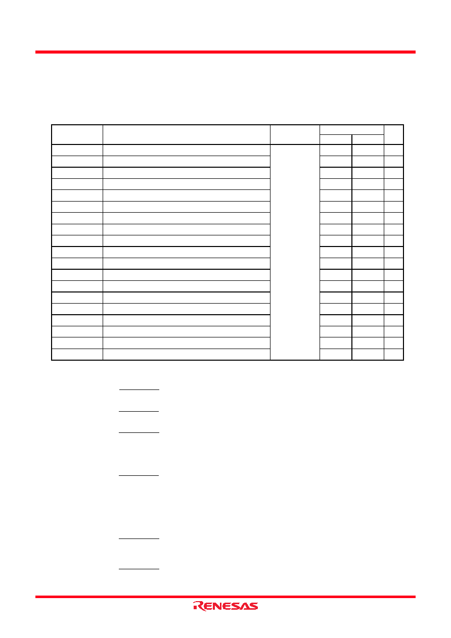
Switching Characteristics
(VCC1 = VCC2 = 3.0 to 3.6 V, VSS = 0 V, Topr = -20 to 85
°C unless otherwise specified)
Table 5.49
Memory Expansion Mode and Microprocessor Mode (when accessing external
memory space with multiplexed bus)
NOTES:
1. Values, which depend on BCLK frequency, can be obtained from the following equations.
2. Values, which depend on BCLK frequency and external bus cycles, can be obtained from the following equation.
3. Values, which depend on BCLK frequency and external bus cycles, can be obtained from the following equation.
4. Values, which depend on BCLK frequency and external bus cycles, can be obtained from the following equation.
5. tc [ns] is added when recovery cycle is inserted.
Symbol
Parameter
Measurement
Condition
Standard
Unit
Min.
Max.
td(BCLK-AD)
Address output delay time
See Figure 5.2
18
ns
th(BCLK-AD)
Address output hold time (BCLK standard)
0
ns
th(RD-AD)
Address output hold time (RD standard)(5)
(note 1)
ns
th(WR-AD)
Address output hold time (WR standard)(5)
(note 1)
ns
td(BCLK-CS)
Chip-select signal output delay time
18
ns
th(BCLK-CS)
Chip-select signal output hold time (BCLK standard)
0
ns
th(RD-CS)
Chip-select signal output hold time (RD standard)(5)
(note 1)
ns
th(WR-CS)
Chip-select signal output hold time (WR standard)(5)
(note 1)
ns
td(BCLK-RD)
RD signal output delay time
18
ns
th(BCLK-RD)
RD signal output hold time
-3
ns
td(BCLK-WR)
WR signal output delay time
18
ns
th(BCLK-WR)
WR signal output hold time
0
ns
td(DB-WR)
Data output delay time (WR standard)
(note 2)
ns
th(WR-DB)
Data output hold time (WR standard)(5)
(note 1)
ns
td(BCLK-ALE)
ALE signal output delay time (BCLK standard)
18
ns
th(BCLK-ALE)
ALE signal output hold time (BCLK standard)
-2
ns
td(AD-ALE)
ALE signal output delay time (address standard)
(note 3)
ns
th(ALE-AD)
ALE signal output hold time (address standard)
(note 4)
ns
tdz(RD-AD)
Address output float start time
8
ns
109
f(BCLK) × 2
- 10 [ns]
th(RD-AD)
=
109
f(BCLK) × 2
- 10 [ns]
th(WR-AD) =
109
f(BCLK) × 2
- 10 [ns]
th(RD-CS)
=
109
f(BCLK) × 2
- 10 [ns]
th(WR-CS) =
109
f(BCLK) × 2
- 15 [ns]
th(WR-DB) =
109 × m
f(BCLK) × 2
- 25 [ns] (if external bus cycle is a
φ + bφ, m = (b × 2) - 1)
td(DB-WR) =
109 × n
f(BCLK) × 2
- 20 [ns] (if external bus cycle is a
φ + bφ, n = a)
td(AD-ALE) =
109 × n
f(BCLK) × 2
- 10 [ns] (if external bus cycle is a
φ + bφ, n = a)
th(ALE-AD) =
VCC1 = VCC2 = 3.3 V
相關(guān)PDF資料 |
PDF描述 |
|---|---|
| M34238MK-XXXGP | 4-BIT, MROM, 4 MHz, MICROCONTROLLER, PDSO20 |
| M34250E2-XXXFP | 4-BIT, OTPROM, 4.4 MHz, MICROCONTROLLER, PDSO20 |
| M34250M2-XXXFP | 4-BIT, MROM, 4.4 MHz, MICROCONTROLLER, PDSO20 |
| M34250M2-XXXFP | 4-BIT, MROM, 4.4 MHz, MICROCONTROLLER, PDSO20 |
| M34280M1-XXXFP | 4-BIT, MROM, 4 MHz, MICROCONTROLLER, PDSO20 |
相關(guān)代理商/技術(shù)參數(shù) |
參數(shù)描述 |
|---|---|
| M308B6FGGP | 制造商:RENESAS 制造商全稱:Renesas Technology Corp 功能描述:RENESAS MCU M16C FAMILY / M32C/80 SERIES |
| M308B6SGP | 制造商:RENESAS 制造商全稱:Renesas Technology Corp 功能描述:RENESAS MCU |
| M308B8FCGP | 制造商:RENESAS 制造商全稱:Renesas Technology Corp 功能描述:RENESAS MCU M16C FAMILY / M32C/80 SERIES |
| M308B8FGGP | 制造商:RENESAS 制造商全稱:Renesas Technology Corp 功能描述:RENESAS MCU |
| M308B8SGP | 制造商:RENESAS 制造商全稱:Renesas Technology Corp 功能描述:RENESAS MCU M16C FAMILY / M32C/80 SERIES |
發(fā)布緊急采購,3分鐘左右您將得到回復(fù)。