- 您現(xiàn)在的位置:買賣IC網(wǎng) > PDF目錄369873 > LV8572AMX Real-Time Clock PDF資料下載
參數(shù)資料
| 型號(hào): | LV8572AMX |
| 英文描述: | Real-Time Clock |
| 中文描述: | 實(shí)時(shí)時(shí)鐘 |
| 文件頁數(shù): | 3/24頁 |
| 文件大小: | 353K |
| 代理商: | LV8572AMX |

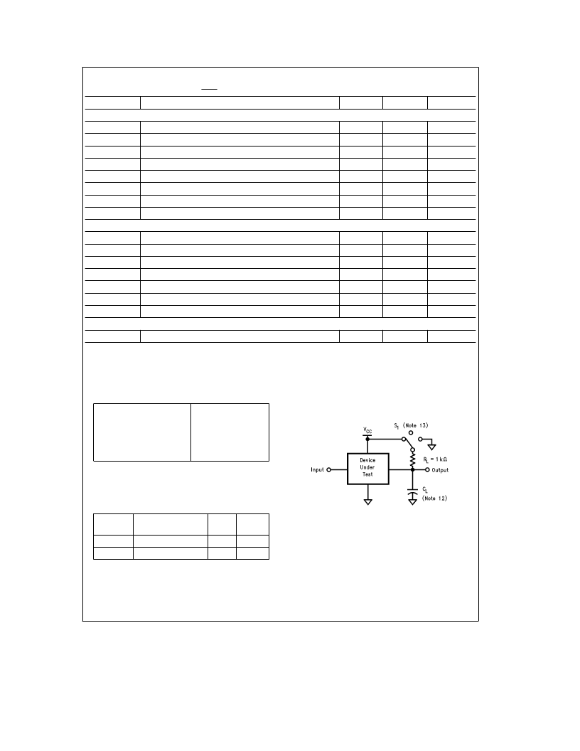
AC Electrical Characteristics
V
CC
e
3.3V
g
10%, V
BB
e
2.5V, V
PFAIL
l
V
IH
, C
L
e
100 pF (unless otherwise specified)
Symbol
Parameter
Min
Max
Units
READ TIMING
t
AR
Address Valid Prior to Read Strobe
10
ns
t
RW
Read Strobe Width (Note 9)
100
ns
t
CD
Chip Select to Data Valid Time
100
ns
t
RAH
Address Hold after Read (Note 10)
2
ns
t
RD
Read Strobe to Valid Data
90
ns
t
DZ
Read or Chip Select to TRI-STATE
80
ns
t
RCH
Chip Select Hold after Read Strobe (Note 10)
0
ns
t
DS
Minimum Inactive Time between Read or Write Accesses
70
ns
WRITE TIMING
t
AW
Address Valid before Write Strobe
10
ns
t
WAH
Address Hold after Write Strobe (Note 10)
2
ns
t
CW
Chip Select to End of Write Strobe
110
ns
t
WW
Write Strobe Width (Note 11)
100
ns
t
DW
Data Valid to End of Write Strobe
70
ns
t
WDH
Data Hold after Write Strobe (Note 10)
2
ns
t
WCH
Chip Select Hold after Write Strobe (Note 10)
0
ns
INTERRUPT TIMING
t
ROLL
Clock rollover to INTR out is typically 20
m
s
Note 9:
Read Strobe width as used in the read timing table is defined as the period when both chip select and read inputs are low. Hence read commences when
both signals are low and terminates when either signal returns high.
Note 10:
Hold time is guaranteed by design but not production tested. This limit is not used to calculate outgoing quality levels.
Note 11:
Write Strobe width as used in the write timing table is defined as the period when both chip select and write inputs are low. Hence write commences when
both signals are low and terminates when either signal returns high.
AC Test Conditions
Input Pulse Levels
Input Rise and Fall Times
Input and Output
Reference Levels
TRI-STATE Reference
Levels (Note 13)
GND to 3.0V
6 ns (10%–90%)
1.3V
Active High
a
0.5V
Active Low
b
0.5V
Note 12:
C
L
e
100 pF, includes jig and scope capacitance.
Note 13:
S1
e
V
CC
for active low to high impedance measurements.
S1
e
GND for active high to high impedance measurements.
S1
e
open for all other timing measurements.
Capacitance
(T
A
e
25
§
C, f
e
1 MHz)
Symbol
Parameter
(Note 14)
Typ
Units
C
IN
Input Capacitance
5
pF
C
OUT
Output Capacitance
7
pF
Note 14:
This parameter is not 100% tested.
Note 15:
Output rise and fall times 25 ns max (10%–90%) with 100 pF load.
TL/F/11416–2
3
相關(guān)PDF資料 |
PDF描述 |
|---|---|
| LV8572AVX | Real-Time Clock |
| LV8800C | Optoelectronic |
| LVA12D | Analog IC |
| LVA12S | Analog IC |
| LVA15D | Analog IC |
相關(guān)代理商/技術(shù)參數(shù) |
參數(shù)描述 |
|---|---|
| LV8572AN | 制造商:Rochester Electronics LLC 功能描述:- Bulk |
| LV8572AVX | 制造商:未知廠家 制造商全稱:未知廠家 功能描述:Real-Time Clock |
| LV8573A | 制造商:NSC 制造商全稱:National Semiconductor 功能描述:LV8573A Low Voltage Real Time Clock (RTC) |
| LV8573AM | 制造商:NSC 制造商全稱:National Semiconductor 功能描述:LV8573A Low Voltage Real Time Clock (RTC) |
| LV8573AN | 制造商:NSC 制造商全稱:National Semiconductor 功能描述:LV8573A Low Voltage Real Time Clock (RTC) |
發(fā)布緊急采購(gòu),3分鐘左右您將得到回復(fù)。