- 您現(xiàn)在的位置:買賣IC網(wǎng) > PDF目錄369873 > LV8572AMX Real-Time Clock PDF資料下載
參數(shù)資料
| 型號: | LV8572AMX |
| 英文描述: | Real-Time Clock |
| 中文描述: | 實時時鐘 |
| 文件頁數(shù): | 15/24頁 |
| 文件大?。?/td> | 353K |
| 代理商: | LV8572AMX |

Functional Description
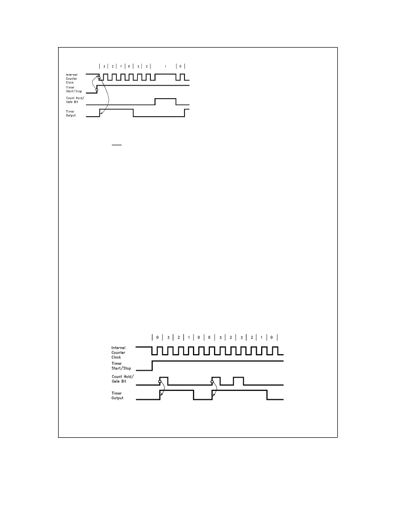
(Continued)
TL/F/11416–14
FIGURE 10. Timing Waveforms for Timer Mode 2
(MFO Output Programmed Active High)
MODE 3: RETRIGGERABLE ONE SHOT
Once the timer Start/Stop bit is set the output stays inac-
tive, and nothing happens until the Count Hold/Gate (CHG)
bit is set in the timer control register. When a transition
ocurs the one shot output is set active immediately; the
counter is loaded with the value in the input register on the
next transition of the input clock and the countdown begins.
If a retrigger occurs, regardless of the current counter value,
the counters will be reloaded with the value in the input
register and the counter will be restarted without changing
the output state. SeeFigure 11. A trigger count can occur at
any time during the count cycle. In this mode the timer will
output a single pulse whose width is determined by the val-
ue in the input data register (N) and the input clock period.
Pulse Width
e
Clock Period
c
N
The timer will generate an interrupt only when it reaches a
count of zero. This timer mode is useful for continuous
‘‘watch dog’’ timing, line frequency power failure detection,
etc.
READING THE TIMERS
National has discovered that some users may encounter
unacceptable error rates for their applications when reading
the timers on the fly asynchronously. When doing asynchro-
nous reads of the timers, an error may occur. The error is
that a successive read may be larger than the previous
read. Experimental results indicate that the typical error rate
is approximately one per 29000 under the following condi-
tions:
Timer clock frequency of 5 MHz.
Computer: 386/33 MHz PC/AT
Program:
Microsoft ‘C’ 6.0, reading and saving timer con-
tents in a continuous loop.
Those users who find the error rate unacceptable may re-
duce the problem effectively to zero by employing a hard-
ware work-around that synchronizes the writing of the read
bit to the timer control register with respect to the decre-
menting clock. Refer to Figure 1 in Appendix A, for a sug-
gested hardware work-around.
A software work-around can reduce the errors but not as
substantial as a hardware work-around. Software work-
arounds are based on observations that the read following a
bad read appeared to be valid.
This problem concerns statistical probability and is similar to
metastability issues. For more information on metastability,
refer to 1991 IEEE transactions on Custom Integrated Cir-
cuits Conference, paper by T.J. Gabara of AT&T Bell Labo-
ratories, page 29.4.1.
Normally reading the timer data register addresses, 0FH
and 10H for Timer 0 and 11H and 12H for Timer 1 will result
in reading the input data register which contains the preset
value for the timers.
To read the contents of a timer, the
m
P first sets the timer
read bit in the appropriate Timer Control Register high. This
will cause the counter’s contents to be latched to 2–8 bit
output registers, and will enable these registers to be read if
the
m
P reads the timer’s input data register addresses. On
reading the LSB byte the timer read bit is internally reset
and subsequent reads of the timer locations will return the
input register values.
DETAILED REGISTER DESCRIPTION
There are 5 external address bits: Thus, the host microproc-
essor has access to 32 locations at one time. An internal
switching scheme provides a total of 67 locations.
This complete address space is organized into two pages.
Page 0 contains two blocks of control registers, timers, real
time clock counters, and special purpose RAM, while page
1 contains general purpose RAM. Using two blocks enables
the 9 control registers to be mapped into 5 locations. The
only register that does not get switched is the Main Status
Register. It contains the page select bit and the register
select bit as well as status information.
A memory map is shown inFigure 2 and register addressing
in Table VII. They show the name, address and page loca-
tions for the LV8571A.
TL/F/11416–15
FIGURE 11. Timing Waveforms for Timer Mode 3, MFO Output Programmed Active High
15
相關(guān)PDF資料 |
PDF描述 |
|---|---|
| LV8572AVX | Real-Time Clock |
| LV8800C | Optoelectronic |
| LVA12D | Analog IC |
| LVA12S | Analog IC |
| LVA15D | Analog IC |
相關(guān)代理商/技術(shù)參數(shù) |
參數(shù)描述 |
|---|---|
| LV8572AN | 制造商:Rochester Electronics LLC 功能描述:- Bulk |
| LV8572AVX | 制造商:未知廠家 制造商全稱:未知廠家 功能描述:Real-Time Clock |
| LV8573A | 制造商:NSC 制造商全稱:National Semiconductor 功能描述:LV8573A Low Voltage Real Time Clock (RTC) |
| LV8573AM | 制造商:NSC 制造商全稱:National Semiconductor 功能描述:LV8573A Low Voltage Real Time Clock (RTC) |
| LV8573AN | 制造商:NSC 制造商全稱:National Semiconductor 功能描述:LV8573A Low Voltage Real Time Clock (RTC) |
發(fā)布緊急采購,3分鐘左右您將得到回復(fù)。