- 您現(xiàn)在的位置:買賣IC網(wǎng) > PDF目錄39399 > LT2435IGN#PBF (LINEAR TECHNOLOGY CORP) 1-CH 20-BIT DELTA-SIGMA ADC, SERIAL ACCESS, PDSO16 PDF資料下載
參數(shù)資料
| 型號(hào): | LT2435IGN#PBF |
| 廠商: | LINEAR TECHNOLOGY CORP |
| 元件分類: | ADC |
| 英文描述: | 1-CH 20-BIT DELTA-SIGMA ADC, SERIAL ACCESS, PDSO16 |
| 封裝: | 0.150 INCH, LEAD FREE, PLASTIC, SSOP-16 |
| 文件頁(yè)數(shù): | 16/40頁(yè) |
| 文件大?。?/td> | 458K |
| 代理商: | LT2435IGN#PBF |
第1頁(yè)第2頁(yè)第3頁(yè)第4頁(yè)第5頁(yè)第6頁(yè)第7頁(yè)第8頁(yè)第9頁(yè)第10頁(yè)第11頁(yè)第12頁(yè)第13頁(yè)第14頁(yè)第15頁(yè)當(dāng)前第16頁(yè)第17頁(yè)第18頁(yè)第19頁(yè)第20頁(yè)第21頁(yè)第22頁(yè)第23頁(yè)第24頁(yè)第25頁(yè)第26頁(yè)第27頁(yè)第28頁(yè)第29頁(yè)第30頁(yè)第31頁(yè)第32頁(yè)第33頁(yè)第34頁(yè)第35頁(yè)第36頁(yè)第37頁(yè)第38頁(yè)第39頁(yè)第40頁(yè)
LTC2435/LTC2435-1
23
24351fb
APPLICATIO S I FOR ATIO
WU
U
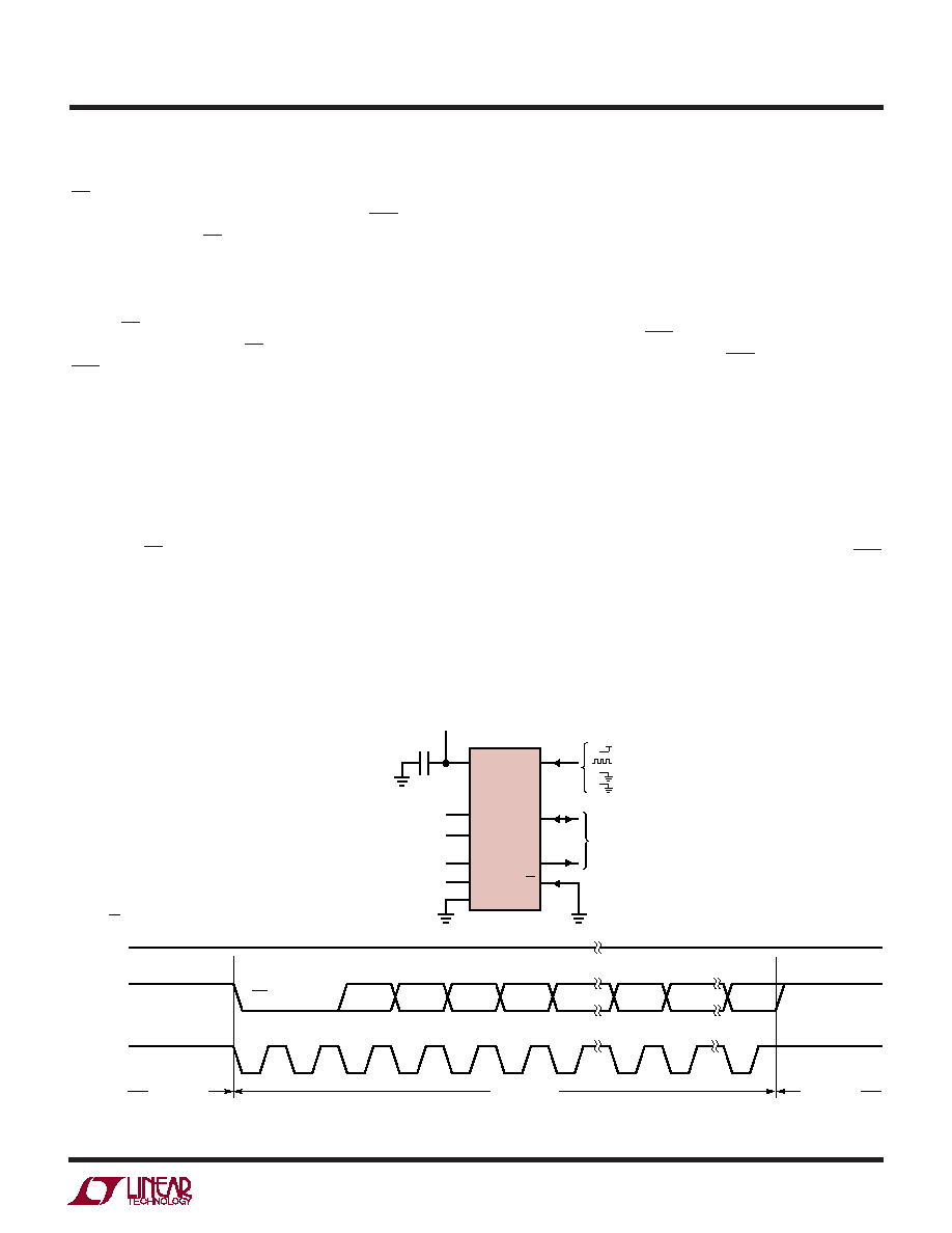
Figure 13. Internal Serial Clock, Continuous Operation
SDO
SCK
(INTERNAL)
CS
LSB
MSB
SIG
BIT 5
BIT 0
BIT 19
BIT 18
BIT 20
BIT 21
BIT 22
EOC
BIT 23
DATA OUTPUT
CONVERSION
2435 F13
VCC
FO
REF+
REF–
SCK
IN+
IN–
SDO
GND
CS
214
3
4
13
5
6
12
1, 7, 8, 9, 10, 15, 16
11
REFERENCE
VOLTAGE
0.1V TO VCC
ANALOG INPUT RANGE
–0.5VREF TO 0.5VREF
2-WIRE
INTERFACE
1
μF
2.7V TO 5.5V
LTC2435/
LTC2435-1
= 50Hz REJECTION (LTC2435)
= EXTERNAL OSCILLATOR
= 60Hz REJECTION (LTC2435)
= 50Hz/60Hz REJECTION (LTC2435-1)
VCC
A similar situation may occur during the sleep state when
CS is pulsed HIGH-LOW-HIGH in order to test the conver-
sion status. If the device is in the sleep state (EOC = 0), SCK
will go LOW. Once CS goes HIGH (within the time period
defined above as tEOCtest), the internal pull-up is activated.
For a heavy capacitive load on the SCK pin, the internal
pull-up may not be adequate to return SCK to a HIGH level
before CS goes low again. This is not a concern under
normal conditions where CS remains LOW after detecting
EOC = 0. This situation is easily overcome by adding an
external 10k pull-up resistor to the SCK pin.
Internal Serial Clock, 2-Wire I/O,
Continuous Conversion
This timing mode uses a 2-wire, all output (SCK and SDO)
interface. The conversion result is shifted out of the device
by an internally generated serial clock (SCK) signal, see
Figure 13. CS may be permanently tied to ground, simpli-
fying the user interface or isolation barrier.
The internal serial clock mode is selected at the end of the
power-on reset (POR) cycle. The POR cycle is concluded
approximately 1ms after VCC exceeds 2.2V. An internal
weak pull-up is active during the POR cycle; therefore, the
internal serial clock timing mode is automatically selected
if SCK is not externally driven LOW (if SCK is loaded such
that the internal pull-up cannot pull the pin HIGH, the
external SCK mode will be selected).
During the conversion, the SCK and the serial data output
pin (SDO) are HIGH (EOC = 1). Once the conversion is
complete, SCK and SDO go LOW (EOC = 0) indicating the
conversion has finished. The data output cycle begins on
the first rising edge of SCK and ends after the 24th rising
edge. Data is shifted out the SDO pin on each falling edge
of SCK. The internally generated serial clock is output to
the SCK pin. This signal may be used to shift the conver-
sion result into external circuitry. EOC can be latched on
the first rising edge of SCK and the last bit of the
conversion result can be latched on the 24th rising edge
of SCK. After the 24th rising edge, SDO goes HIGH (EOC
= 1) indicating a new conversion is in progress. SCK
remains HIGH during the conversion.
相關(guān)PDF資料 |
PDF描述 |
|---|---|
| LT280A | SPECIALTY ANALOG CIRCUIT, PDSO4 |
| LT3407IDD-2 | 1.6 A DUAL SWITCHING CONTROLLER, 2700 kHz SWITCHING FREQ-MAX, PDSO10 |
| LT3407IMSE-2#PBF | 1.6 A DUAL SWITCHING CONTROLLER, 2700 kHz SWITCHING FREQ-MAX, PDSO10 |
| LT3407IDD-2#TRPBF | 1.6 A DUAL SWITCHING CONTROLLER, 2700 kHz SWITCHING FREQ-MAX, PDSO10 |
| LT3407IMSE-2#TRPBF | 1.6 A DUAL SWITCHING CONTROLLER, 2700 kHz SWITCHING FREQ-MAX, PDSO10 |
相關(guān)代理商/技術(shù)參數(shù) |
參數(shù)描述 |
|---|---|
| LT24512-15E | 制造商:未知廠家 制造商全稱:未知廠家 功能描述:Analog IC |
| LT2462-SERIES | 制造商:未知廠家 制造商全稱:未知廠家 功能描述:Optoelectronic |
| LT2462XX-SERIES | 制造商:未知廠家 制造商全稱:未知廠家 功能描述:Optoelectronic |
| LT24701DBB#PBF | 制造商:IC'S/TRANSISTORS/DIO 功能描述: 制造商:IC'S/TRANSISTORS/DIODES 功能描述: |
| LT24DP | 制造商:UNBRANDED 功能描述:24MM SWIFT SPLICE LEADER TAPE (2000/BX) |
發(fā)布緊急采購(gòu),3分鐘左右您將得到回復(fù)。